Datasheet Details
| Part number | AO6420 |
|---|---|
| Manufacturer | Alpha & Omega Semiconductors |
| File Size | 270.23 KB |
| Description | 60V N-Channel MOSFET |
| Download | AO6420 Download (PDF) |
|
|
| Part number | AO6420 |
|---|---|
| Manufacturer | Alpha & Omega Semiconductors |
| File Size | 270.23 KB |
| Description | 60V N-Channel MOSFET |
| Download | AO6420 Download (PDF) |
|
|
|
The AO6420 uses advanced trench technology to provide excellent RDS(ON) and low gate charge.
This device is suitable for use as a load switch or in PWM applications.
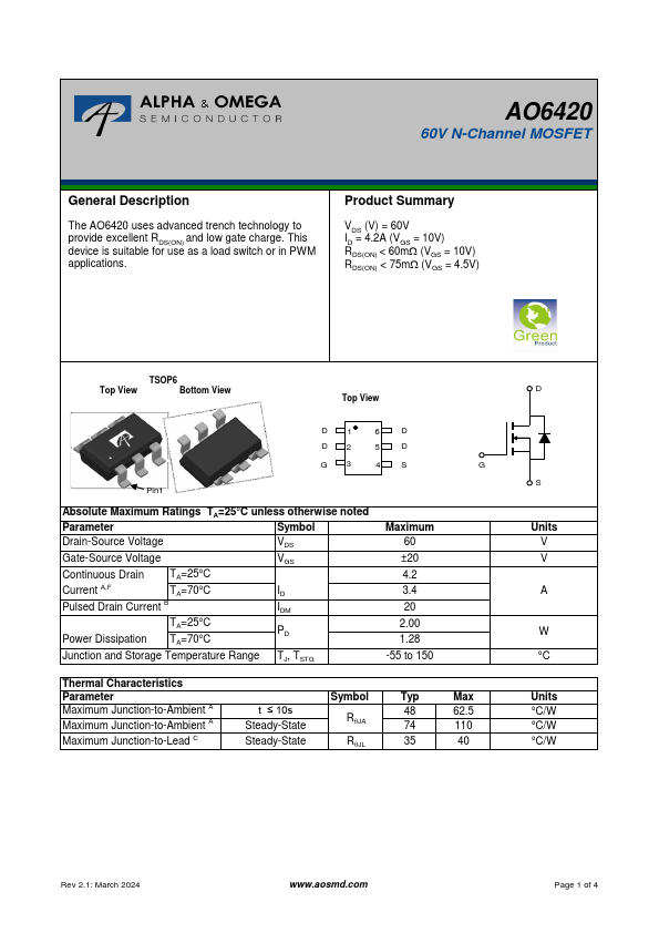
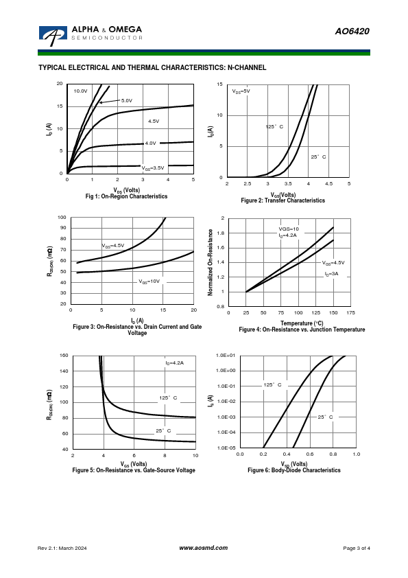
Product Summary VDS (V) = 60V ID = 4.2A (VGS = 10V) RDS(ON) < 60mW (VGS = 10V) RDS(ON) < 75mW (VGS = 4.5V) TSOP6 Top View Bottom View Top View D1 6 D D2 5D G3 4S G Pin1 Absolute Maximum Ratings TA=25°C unless otherwise noted Parameter Symbol Drain-Source Voltage VDS Gate-Source Voltage VGS Continuous Drain TA=25°C Current A,F TA=70°C ID Pulsed Drain Current B IDM Power Dissipation TA=25°C TA=70°C PD Junction and Storage Temperature Range TJ, TSTG Maximum 60 ±20 4.2 3.4 20 2.00 1.28 -55 to 150 Thermal Characteristics Parameter Symbol Typ Max Maximum Junction-to-Ambient A Maximum Junction-to-Ambient A t ≤ 10s Steady-State RqJA 48 74 62.5 110 Maximum Junction-to-Lead C Steady-State RqJL 35 40 D S Units V V A W °C Units °C/W °C/W °C/W Rev 2.1: March 2024 www.aosmd.com Page 1 of 4 AO6420 N Channel Electrical Characteristics (TJ=25°C unless otherwise noted) Symbol Parameter Conditions Min Typ Max Units STATIC PARAMETERS BVDSS Drain-Source Breakdown Voltage ID=250mA, VGS=0V 60 V IDSS Zero Gate Voltage Drain Current VDS=60V, VGS=0V TJ=55°C 1 mA 5 IGSS Gate-Body leakage current VDS=0V, VGS= ±20V 100 nA VGS(th) Gate Threshold Voltage VDS=VGS ID=250mA 1 2.3 3 V ID(ON) On state drain current VGS=10V, VDS=5V 20 A RDS(ON) Static Drain-Source On-Resistance VGS=10V, ID=4.2A TJ=125°C 50 60 mW 85 VGS=4.5V, ID=3A 60 75 mW gFS Forward Transconductance VDS=5V, ID=4.2A 13 S VSD Diode Forward Voltage IS=1A,VGS=0V 0.78 1 V IS Maximum Body-Diode Continuous Current 3 A DYNAMIC PARAMETERS Ciss Input Capacitance Coss Output Capacitance Crss Reverse Transfer Capacitance Rg Gate resistance VGS=0V, VDS=30V, f=1MHz VGS=0V, VDS=0V, f=1MHz 450 540 pF 60 pF 25 pF 1.65 2 W
AO6420 60V N-Channel MOSFET General.
| Brand Logo | Part Number | Description | Manufacturer |
|---|---|---|---|
| AO6420 | N-Channel MOSFET | Kexin |
| Part Number | Description |
|---|---|
| AO6422 | 20V N-Channel MOSFET |
| AO6424 | 30V N-Channel MOSFET |
| AO6424A | N-Channel MOSFET |
| AO6400 | 30V N-Channel MOSFET |
| AO6401 | 30V P-Channel MOSFET |
| AO6401A | P-Channel MOSFET |
| AO6402 | 30V N-Channel MOSFET |
| AO6402A | 30V N-Channel MOSFET |
| AO6402L | N-Channel MOSFET |
| AO6403 | 30V P-Channel MOSFET |