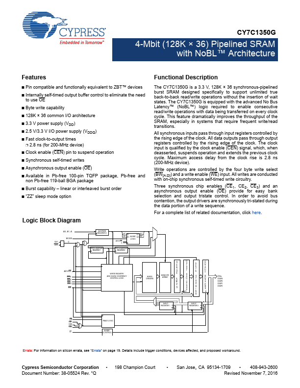
CY7C1350G Overview
The CY7C1350G is a 3.3 V, 128K × 36 synchronous-pipelined burst SRAM designed specifically to support unlimited true back-to-back read/write operations without the inserti.
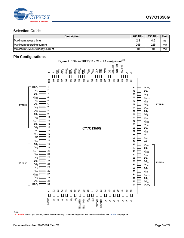
CY7C1350G Key Features
- Pin patible and functionally equivalent to ZBT™ devices
- Internally self-timed output buffer control to eliminate the need
- Byte write capability
- 128K × 36 mon I/O architecture
- 3.3 V power supply (VDD)
- 2.5 V/3.3 V I/O power supply (VDDQ)
- Fast clock-to-output times
- 2.8 ns (for 200-MHz device)
- Clock enable (CEN) pin to suspend operation
- Synchronous self-timed writes