Datasheet4U Logo Datasheet4U.com

M15F2G16128A-DEBG2L Datasheet DDR3 SDRAM

Manufacturer: ESMT (Elite Semiconductor Microelectronics Technology)

Download the M15F2G16128A-DEBG2L datasheet PDF. This datasheet also includes the M15F2G16128A variant, as both parts are published together in a single manufacturer document.

📥 Download Datasheet

Note: The manufacturer provides a single datasheet file (M15F2G16128A-ESMT.pdf) that lists specifications for multiple related part numbers.

General Description

The 2Gb Double-Data-Rate-3 (DDR3) DRAM is double data rate architecture to achieve high-speed operation.

It is internally configured as an eight bank DRAMs.

The 2Gb chip is organized as 16Mbit x 16 I/Os x 8 bank devices.

Overview

ESMT DR3 SDRAM Feature  
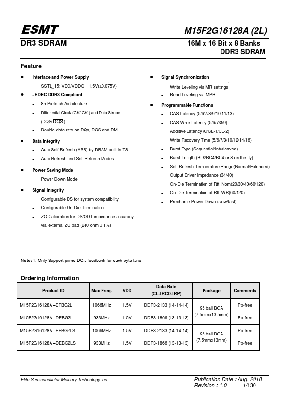
Interface and Power Supply ˗ SSTL_15: VDD/VDDQ = 1.5V(±0.075V)  JEDEC DDR3 Compliant ˗ 8n Prefetch Architecture ˗ Differential Clock (CK/ CK ) and Data Strobe (DQS/ DQS ) ˗ Double-data rate on DQs, DQS and DM  Data Integrity ˗ Auto Self Refresh (ASR) by DRAM built-in TS ˗ Auto Refresh and Self Refresh Modes  Power Saving Mode ˗ Power Down Mode  Signal Integrity ˗ Configurable DS for system compatibility ˗ Configurable On-Die Termination ˗ ZQ Calibration for DS/ODT impedance accuracy via external ZQ pad (240 ohm ± 1%) M15F2G16128A (2L) 16M x 16 Bit x 8 Banks DDR3 SDRAM  Signal Synchronization 1 ˗ Write Leveling via MR settings ˗ Read Leveling via MPR  Programmable Functions ˗ CAS Latency (5/6/7/8/9/10/11/13) ˗ CAS Write Latency (5/6/7/8/9) ˗ Additive Latency (0/CL-1/CL-2) ˗ Write Recovery Time (5/6/7/8/10/12/14/16) ˗ Burst Type (Sequential/Interleaved) ˗ Burst Length (BL8/BC4/BC4 or 8 on the fly) ˗ Self Refresh Temperature Range(Normal/Extended) ˗ Output Driver Impedance (34/40) ˗ On-Die Termination of Rtt_Nom(20/30/40/60/120) ˗ On-Die Termination of Rtt_WR(60/120) ˗ Precharge Power Down (slow/fast) Note: 1.

Only Support prime DQ’s feedback for each byte lane.

Ordering Information Product ID M15F2G16128A –EFBG2L M15F2G16128A –DEBG2L M15F2G16128A –EFBG2LS M15F2G16128A –DEBG2LS Max Freq.

Key Features

  • and all of the control and address inputs are synchronized with a pair of externally supplied differential clocks. Inputs are latched at the cross point of differential clocks (CK rising and CK falling). All I/Os are synchronized with a single ended DQS or differential DQS pair in a source synchronous fashion. These devices operate with a single 1.5V ± 0.075V power supply and are available in BGA packages. DDR3 SDRAM Addressing Configuration 128Mb x16 # of Bank 8 Bank Address BA0.