EMB17A03V Overview
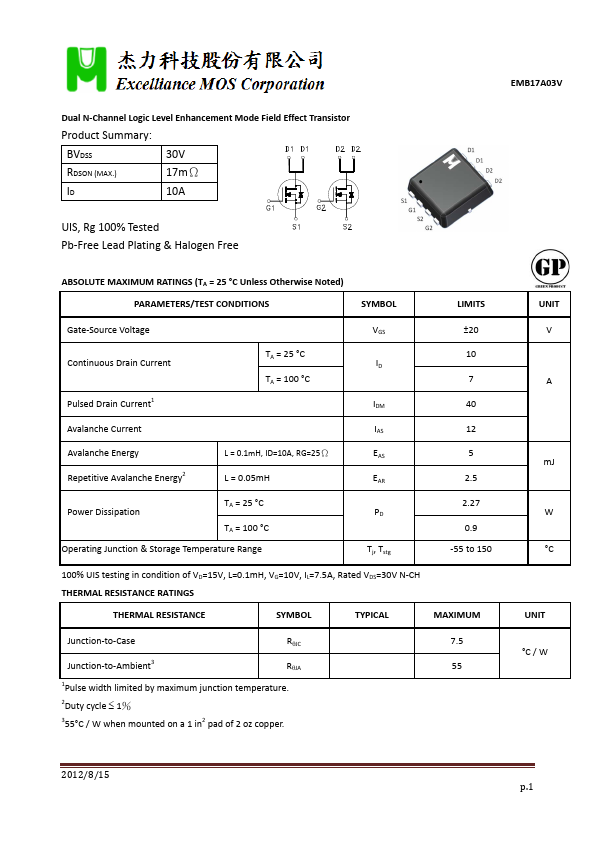
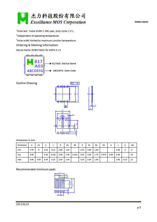
Dual N‐Channel Logic Level Enhancement Mode Field Effect Transistor Product Summary: 2Duty cycle 1% 355°C / W when mounted on a 1 in2 pad of 2 oz copper. Pulse Width 300 sec, Duty Cycle 2%.
| Part number | EMB17A03V |
|---|---|
| Datasheet | EMB17A03V-ExcellianceMOS.pdf |
| File Size | 180.96 KB |
| Manufacturer | Excelliance MOS |
| Description | Dual N-Channel MOSFET |
|
|
Dual N‐Channel Logic Level Enhancement Mode Field Effect Transistor Product Summary: 2Duty cycle 1% 355°C / W when mounted on a 1 in2 pad of 2 oz copper. Pulse Width 300 sec, Duty Cycle 2%.
See all Excelliance MOS datasheets
| Part Number | Description |
|---|---|
| EMB17A03G | Dual N-Channel Logic Level Enhancement Mode Field Effect Transistor |
| EMB17A03H | MOSFET |
| EMB17C03G | N & P-Channel Logic Level Enhancement Mode Field Effect Transistor |
| EMB17N03G | N-Channel Logic Level Enhancement Mode Field Effect Transistor |
| EMB11A03G | MOSFET |
| EMB12K03GP | MOSFET |
| EMB12K03V | MOSFET |
| EMB12N03A | MOSFET |
| EMB12N03G | N-Channel Logic Level Enhancement Mode Field Effect Transistor |
| EMB12N03H | MOSFET |