Datasheet Details
| Part number | FIN1002 |
|---|---|
| Manufacturer | Fairchild Semiconductor (now onsemi) |
| File Size | 1.00 MB |
| Description | LVDS 1-Bit High Speed Differential Receiver |
| Datasheet |
 FIN1002 Datasheet FIN1002 Datasheet
|
|
|
This page provides the datasheet information for the FIN1002, a member of the FIN LVDS 1-Bit High Speed Differential Receiver family.
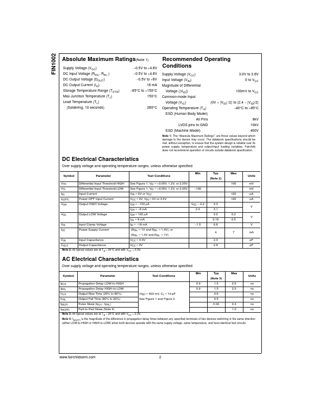
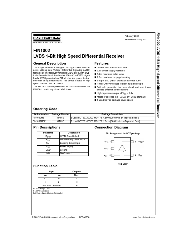
This single receiver is designed for high speed interconnects utilizing Low Voltage Differential Signaling (LVDS) technology.
The receiver translates LVDS levels, with a typical differential input threshold of 100 mV, to LVTTL signal levels.
| Part number | FIN1002 |
|---|---|
| Manufacturer | Fairchild Semiconductor (now onsemi) |
| File Size | 1.00 MB |
| Description | LVDS 1-Bit High Speed Differential Receiver |
| Datasheet |
FIN1002 Datasheet
|
|
|
|