FDV303N
Description
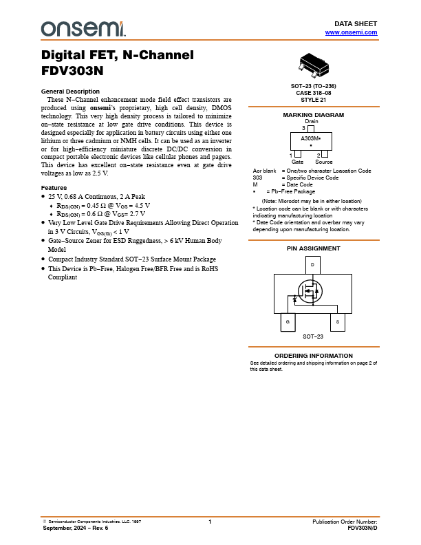
These N-Channel enhancement mode field effect transistors are produced using onsemi’s proprietary, high cell density, DMOS technology. This very high density process is tailored to minimize on-state resistance at low gate drive conditions.
Key Features
- 25 V, 0.68 A Continuous, 2 A Peak
- RDS(ON) = 0.45 Ω @ VGS = 4.5 V
- RDS(ON) = 0.6 Ω @ VGS= 2.7 V
- Very Low Level Gate Drive Requirements Allowing Direct Operation in 3 V Circuits, VGS(th) < 1 V
- Gate-Source Zener for ESD Ruggedness, > 6 kV Human Body Model
- Compact Industry Standard SOT-23 Surface Mount Package
- This Device is Pb-Free, Halogen Free/BFR Free and is RoHS Compliant