NB7VQ572M Key Features
- Input Data Rate > 10 Gb/s Typical
- Data Dependent Jitter < 10 ps
- Maximum Input Clock Frequency > 6 GHz Typical
- Random Clock Jitter < 0.8 ps RMS
- Low Skew 1:2 CML Outputs, < 15 ps max
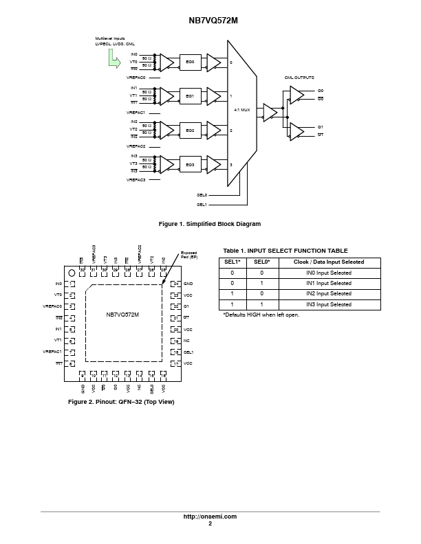
- 4:1 Multi-Level Mux Inputs, accepts LVPECL, CML
- 175 ps Typical Propagation Delay
- 45 ps Typical Rise and Fall Times
- Differential CML Outputs, 400 mV Peak-to-Peak
- Operating Range: VCC = 1.71 V to 3.6 V with GND =