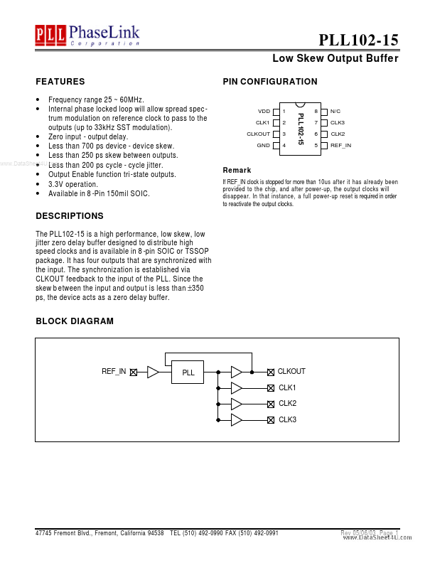
PLL102-15 Description
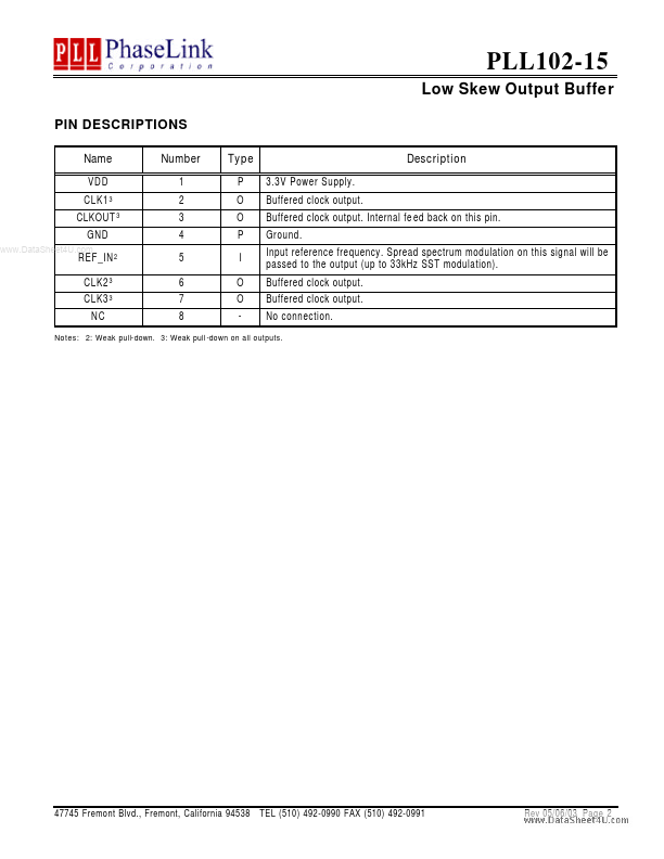
Internal fe ed back on this pin. Input reference frequency. Spread spectrum modulation on this signal will be passed to the output (up to 33kHz SST modulation).
PLL102-15 Key Features
- Zero input
- output delay
- Less than 700 ps device
- device skew
- Less than 250 ps skew between outputs
- Less than 200 ps cycle
- cycle jitter
- Output Enable function tri -state outputs
- 3.3V operation
- Available in 8 -Pin 150mil SOIC