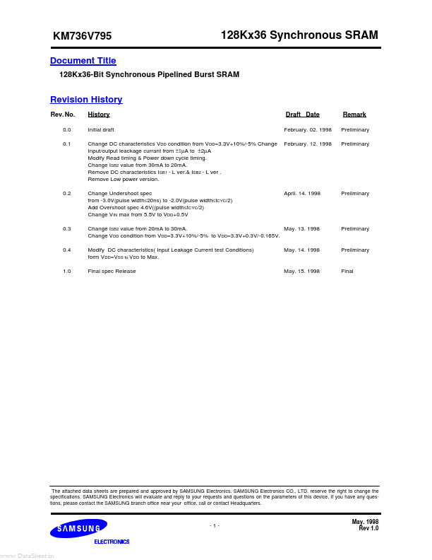
Datasheet4U Logo Datasheet4U.com

KM736V795 Datasheet 128kx36 Synchronous Sram

Manufacturer: Samsung Semiconductor

Overview: KM736V795 Document Title 128Kx36 Synchronous SRAM 128Kx36-Bit Synchronous Pipelined Burst SRAM Revision History Rev. No. 0.0 0.1 History Initial draft Change DC characteristics VDD condition from VDD=3.3V+10%/-5% Change Input/output leackage currant from ±1µA to ±2µA Modify Read timing & Power down cycle timing. Change ISB2 value from 30mA to 20mA. Remove DC characteristics ISB1 - L ver.& ISB2 - L ver . Remove Low power version. Change Undershoot spec from -3.0V(pulse width≤20ns) to -2.0V(pulse width≤tCYC/2) Add Overshoot spec 4.6V((pulse width≤tCYC/2) Change VIN max from 5.5V to VDD+0.5V Draft Date February. 02. 1998 February. 12. 1998 Remark Preliminary Preliminary 0.2 April. 14. 1998 Preliminary 0.3 May. 13. 1998 Change ISB2 value from 20mA to 30mA. Change VDD condition from VDD=3.3V+10%/-5% to VDD=3.3V+0.3V/-0.165V. Modify DC characteristics( Input Leakage Current test Conditions) form VDD=VSS to VDD to Max. Final spec Release May. 14. 1998 Preliminary 0.4 Preliminary 1.0 May. 15. 1998 Final The attached data sheets are prepared and approved by SAMSUNG Electronics. SAMSUNG Electronics CO., LTD. reserve the right to change the specifications. SAMSUNG Electronics will evaluate and reply to your requests and questions on the parameters of this device. If you have any questions, please contact the SAMSUNG branch office near your office, call or contact Headquarters. -1- May. 1998 Rev 1.0 www.DataSheet.

Key Features

  • Synchronous Operation.
  • 2 Stage Pipelined operation with 4 Burst.
  • On-Chip Address Counter.
  • Self-Timed Write Cycle.
  • On-Chip Address and Control Registers.
  • VDD= 3.3V+0.3V/-0.165V Power Supply.
  • I/O Supply Voltage 2.5V+0.4V/-0.13V.
  • 5V Tolerant Inputs Except I/O Pins.
  • Byte Writable Function.
  • Global Write Enable Controls a full bus-width write.
  • Power Down State via ZZ Signal.
  • LBO Pin.

KM736V795 Distributor