K7B401825B Overview
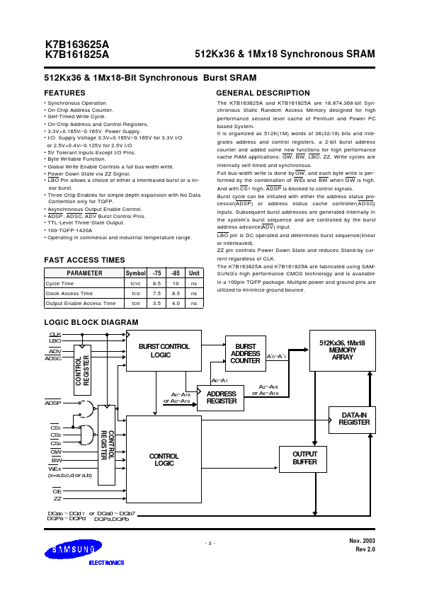
The K7B163625A and K7B161825A are 18,874,368-bit Synchronous Static Random Access Memory designed for high performance second level cache of Pentium and Power PC based System. It is organized as 512K(1M) words of 36(32/18) bits and integrates address and control registers, a 2-bit burst address counter and added some new functions for high performance cache RAM applications; Write cycles are internally self-timed...
K7B401825B Key Features
- Synchronous Operation
- On-Chip Address Counter
- Self-Timed Write Cycle
- On-Chip Address and Control Registers
- 3.3V+0.165V/-0.165V Power Supply
- 5V Tolerant Inputs Except I/O Pins
- Byte Writable Function
- Global Write Enable Controls a full bus-width write
- Power Down State via ZZ Signal
- LBO Pin allows a choice of either a interleaved burst or a linear burst