Datasheet4U Logo Datasheet4U.com

AS7C251MNTF36A - (AS7C251MNTF32A / AS7C251MNTF36A) 2.5V 1M x 32/36 Flowthrough SRAM

This page provides the datasheet information for the AS7C251MNTF36A, a member of the AS7C251MNTF32A (AS7C251MNTF32A / AS7C251MNTF36A) 2.5V 1M x 32/36 Flowthrough SRAM family.

Description

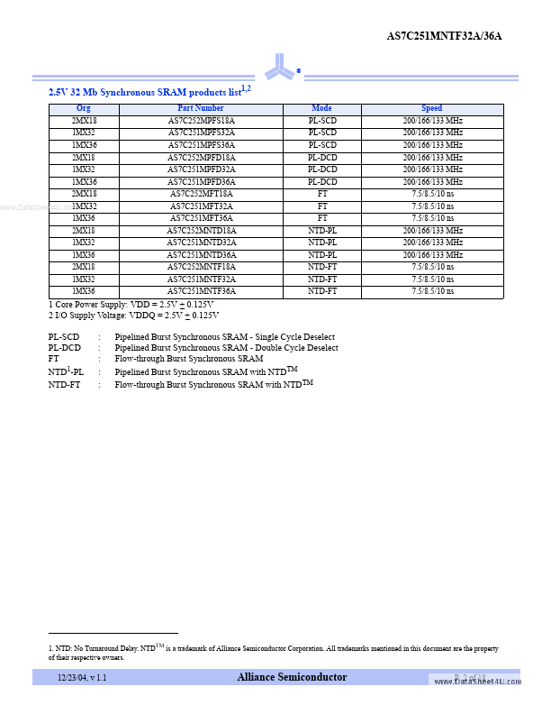
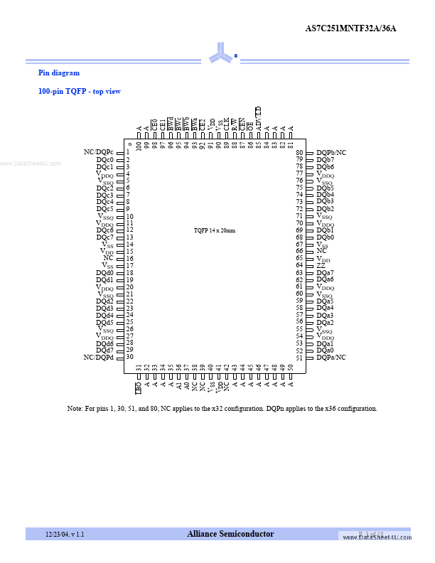
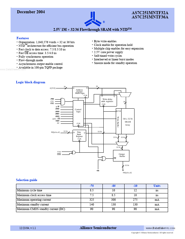
The AS7C251MNTF32A/36A family is a high performance CMOS 32 Mbit synchronous Static Random Access Memory (SRAM) organized as 1,048,576 words × 32 or 36 bits and incorporates a LATE Write.

Features

  • Organization: 1,048,576 words × 32 or 36 bits NTD™architecture for efficient bus operation Fast clock to data access: 7.5/8.5/10 ns Fast OE access time: 3.5/4.0 ns Fully synchronous operation Flow-through mode Asynchronous output enable control Available in 100-pin TQFP package.
  • Byte write enables Clock enable for operation hold Multiple chip enab.

📥 Download Datasheet

Datasheet preview – AS7C251MNTF36A

Datasheet Details

Part number AS7C251MNTF36A
Manufacturer Alliance Semiconductor Corporation
File Size 459.45 KB
Description (AS7C251MNTF32A / AS7C251MNTF36A) 2.5V 1M x 32/36 Flowthrough SRAM
Datasheet download datasheet AS7C251MNTF36A Datasheet
Additional preview pages of the AS7C251MNTF36A datasheet.
Other Datasheets by Alliance Semiconductor Corporation

Full PDF Text Transcription

Click to expand full text
December 2004 ® AS7C251MNTF32A AS7C251MNTF36A 2.5V 1M × 32/36 Flowthrough SRAM with NTDTM Features • • • • • • • • Organization: 1,048,576 words × 32 or 36 bits NTD™architecture for efficient bus operation Fast clock to data access: 7.5/8.5/10 ns Fast OE access time: 3.5/4.0 ns Fully synchronous operation Flow-through mode Asynchronous output enable control Available in 100-pin TQFP package • • • • • • • Byte write enables Clock enable for operation hold Multiple chip enables for easy expansion 2.5V core power supply Self-timed write cycles Interleaved or linear burst modes Snooze mode for standby operation www.DataSheet4U.com Logic block diagram A[19:0] 20 D Address register Burst logic Q 20 CLK CE0 CE1 CE2 R/W BWa BWb BWc BWd ADV / LD LBO ZZ D Q 20 Write delay addr.
Published: |