Description
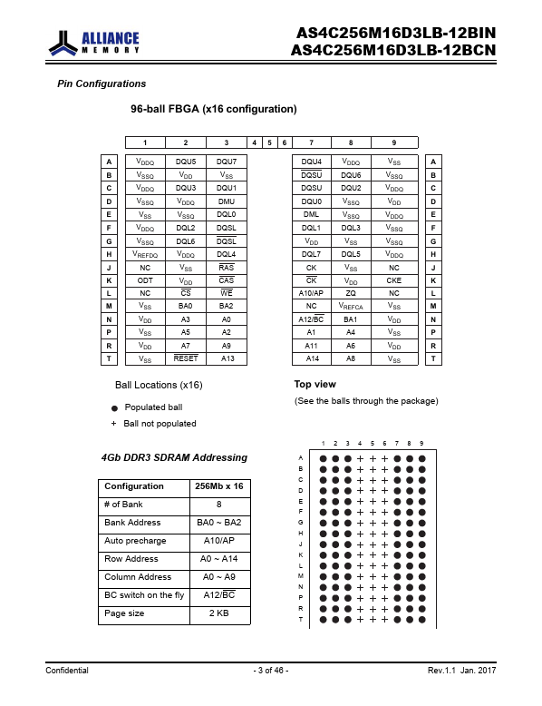
Pin
CK, CK CKE
CS ODT
RAS, CAS, WE DM
(DMU), (DML)
Type
Input Input
Input Input
Input Input
Function
Clock : CK and CK are differential clock inputs.All address and control input signals are sampled on the crossing of the positive edge of CK and negative edge of CK.Output (read) data is referenced to the crossings of CK and CK
Clock Enable : CKE HIGH activates, and CKE Low deactivates, internal clock signals and device input buffers and output drivers.Taking CKE Low provides Precharge Powe
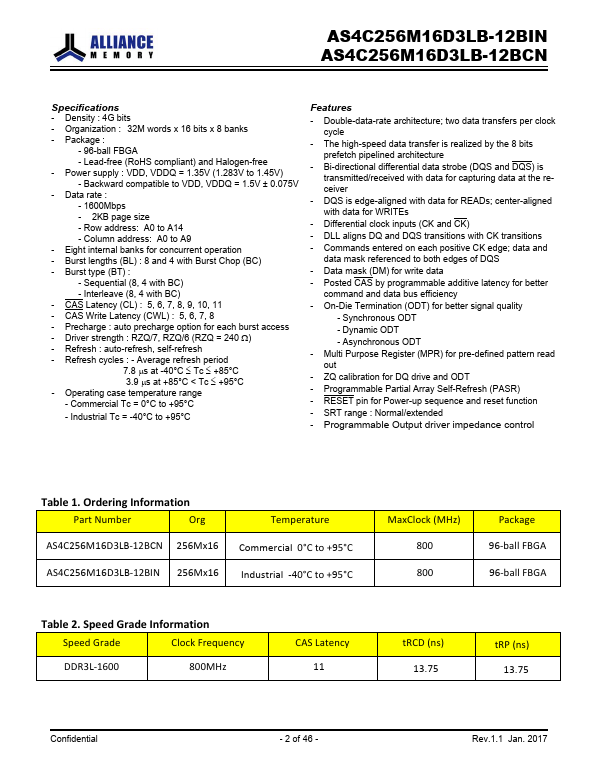
Features
- - Double-data-rate architecture; two data transfers per clock cycle
- The high-speed data transfer is realized by the 8 bits prefetch pipelined architecture
- Bi-directional differential data strobe (DQS and DQS) is transmitted/received with data for capturing data at the receiver
- DQS is edge-aligned with data for READs; center-aligned with data for WRITEs
- Differential clock inputs (CK and CK) - DLL aligns DQ and DQS transitions with CK transitions - Commands entered on each positive CK edge.
 AS4C256M16D3LB-12BIN-AllianceSemiconductor.pdf