Datasheet4U Logo Datasheet4U.com

CY7C147 Datasheet - Cypress Semiconductor

CY7C147 4K x 1 STATIC RAM

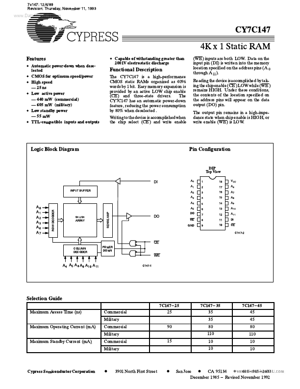
(WE) inputs are both LOW. Data on the input pin (DI) is written into the memory location specified on the address pins (A 0 through A 11). Readingthedeviceisaccomplished bytakĆ ingthechipenable(CE)LOWwhile(WE) remains HIGH. Under these conditions, the contents of the location specified on the addre.

CY7C147 Features

* D D D D D D D Automatic powerĆdown when deseĆ lected CMOS for optimum speed/power High speed Capable of withstanding greater than 2001V electrostatic discharge Ċ 25 ns Low active power Ċ 440 mW (commercial) Ċ 605 mW (military) Low standby power Ċ 55 mW TTLĆcompatible inputs and outputs The CY

CY7C147 Datasheet (407.33 KB)

Preview of CY7C147 PDF

Datasheet Details

Part number:

CY7C147

Manufacturer:

Cypress Semiconductor

File Size:

407.33 KB

Description:

4k x 1 static ram.

📁 Related Datasheet

CY7C140 1K x 8 Dual-Port Static Ram (Cypress Semiconductor)

CY7C140 1K x 8 Dual-Port Static RAM (Cypress Semiconductor)

CY7C141 1K x 8 Dual-Port Static RAM (Cypress Semiconductor)

CY7C1410AV18 (CY7C14xxAV18) 36-Mbit QDR-II SRAM 2-Word Burst Architecture (Cypress Semiconductor)

CY7C1410JV18 (CY7C14xxJV18) SRAM 2-Word Burst Architecture (Cypress Semiconductor)

CY7C1410V18 (CY7C14xxV18) SRAM 2-Word Burst Architecture (Cypress Semiconductor)

CY7C1411AV18 (CY7C14xxAV18) 36-Mbit QDR-II SRAM 4-Word Burst Architecture (Cypress Semiconductor)

CY7C1411BV18 (CY7C14xxBV18) 36-Mbit QDR-II SRAM 4-Word Burst Architecture (Cypress Semiconductor)

CY7C1411JV18 (CY7C14xxJV18) 36-Mbit QDR-II SRAM 4-Word Burst Architecture (Cypress Semiconductor)

CY7C1411KV18 36-Mbit QDR II SRAM Four-Word Burst Architecture (Cypress Semiconductor)

TAGS

CY7C147 STATIC RAM Cypress Semiconductor

Image Gallery

CY7C147 Datasheet Preview Page 2 CY7C147 Datasheet Preview Page 3

CY7C147 Distributor