Datasheet Details
| Part number | M13S128324A |
|---|---|
| Manufacturer | ESMT |
| File Size | 1.72 MB |
| Description | Double Data Rate SDRAM |
| Datasheet |
 M13S128324A-ESMT.pdf M13S128324A-ESMT.pdf
|
| Part number | M13S128324A |
|---|---|
| Manufacturer | ESMT |
| File Size | 1.72 MB |
| Description | Double Data Rate SDRAM |
| Datasheet |
M13S128324A-ESMT.pdf
|
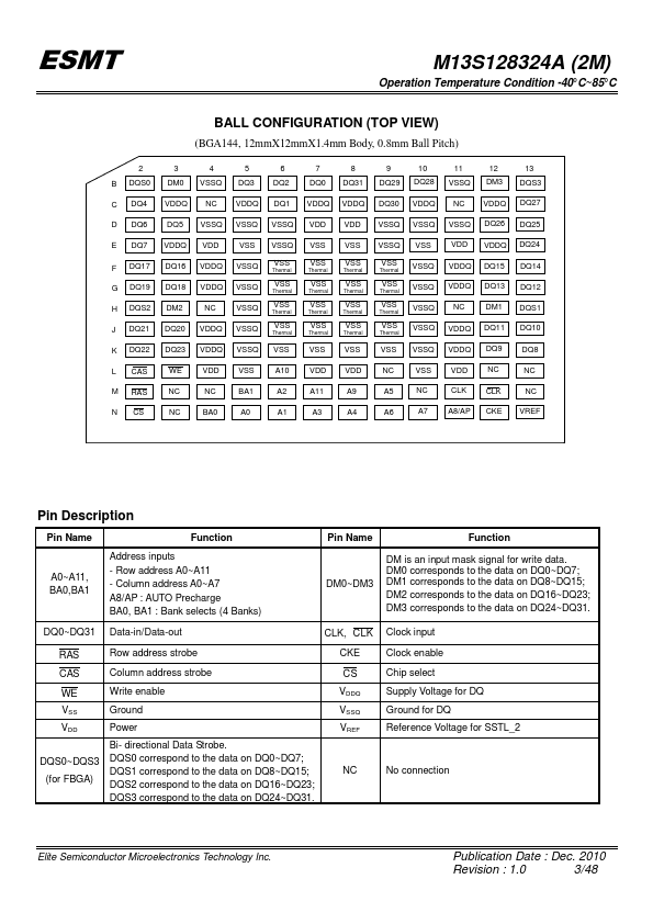
Pin Name Function Pin Name Function A0~A11, BA0,BA1 Address inputs - Row address A0~A11 - Column address A0~A7 A8/AP : AUTO Precharge BA0, BA1 : Bank selects (4 Banks) DM0~DM3 DM is an input mask signal for write data.DM0 corresponds to the data on DQ0~DQ7; DM1 corresponds to the data on DQ8~DQ15; DM2 corresponds to the data on DQ16~DQ23; DM3 corresponds to the data on DQ24~DQ31. DQ0~DQ31 Data-in/Data-out CLK, CLK Clock input RAS Row address strobe CAS Column address strobe WE W
📁 M13S128324A Similar Datasheet