Description
(M13S256328A)
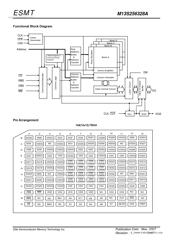
Pin Name Function Address inputs - Row address A0~A11 - Column address A0~A7, A9 A8/AP : AUTO Precharge BA0, BA1 : Bank selects (4 Banks) Data-in/Data-out Row address strobe Column address strobe Write enable Ground Power Bi- directional Data Strobe.DQS0 correspond to the data on DQ0~DQ7. DQS1 correspond to the data on DQ8~DQ15. DQS2 correspond to the data on DQ16~DQ23. DQS3 correspond to the data on DQ24~DQ31. Pin Name
M13S256328A
Function
A0~A11, BA0,BA1
DM0~DM3
DQ Mask ena
Features
- z z z z z z z z z z z z z z z z z z z z z
M13S256328A
2M x 32 Bit x 4 Banks Double Data Rate SDRAM
JEDEC Standard Internal pipelined double-data-rate architecture, two data access per clock cycle Bi-directional data strobe (DQS) On-chip DLL Differential clock inputs (CLK and CLK ) DLL aligns DQ and DQS transition with CLK transition Quad bank operation CAS Latency : 2; 2.5; 3 Burst Type : Sequential and Interleave Burst Length : 2, 4, 8, full page Full page burst length for sequential burst ty.

 M13S256328A_EliteSemiconductorMemoryTechnology.pdf