Description
(M13S32321A)
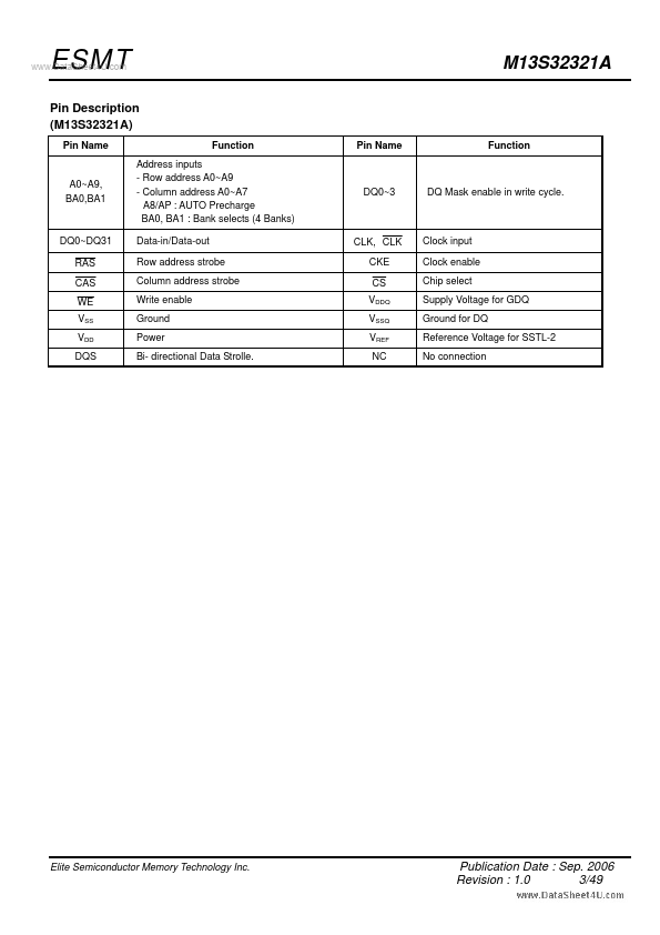
Pin Name Function Address inputs - Row address A0~A9 - Column address A0~A7 A8/AP : AUTO Precharge BA0, BA1 : Bank selects (4 Banks) Data-in/Data-out Row address strobe Column address strobe Write enable Ground Power Bi- directional Data Strolle.Pin Name
M13S32321A
Function
A0~A9, BA0,BA1
DQ0~3
DQ Mask enable in write cycle.DQ0~DQ31 RAS CAS
WE
CLK, CLK CKE CS VDDQ VSSQ VREF NC
Clock input Clock enable Chip select Supply Voltage for GDQ Ground for DQ Reference Voltage for S
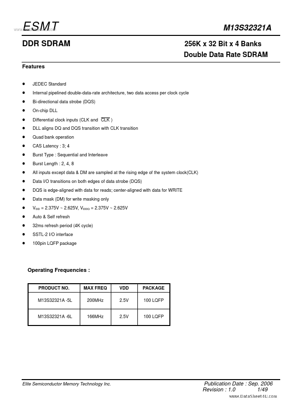
Features
- z z z z z z z z z z z z z z z z z z z
M13S32321A
256K x 32 Bit x 4 Banks Double Data Rate SDRAM
JEDEC Standard Internal pipelined double-data-rate architecture, two data access per clock cycle Bi-directional data strobe (DQS) On-chip DLL Differential clock inputs (CLK and CLK ) DLL aligns DQ and DQS transition with CLK transition Quad bank operation CAS Latency : 3; 4 Burst Type : Sequential and Interleave Burst Length : 2, 4, 8 All inputs except data & DM are sampled at the rising edge of the.
 M13S32321A_EliteSemiconductorMemoryTechnology.pdf