Datasheet Details
| Part number | M13S128168A |
|---|---|
| Manufacturer | Elite Semiconductor Memory Technology |
| File Size | 1.76 MB |
| Description | Double Data Rate SDRAM |
| Datasheet |
 M13S128168A_EliteSemiconductorMemoryTechnology.pdf M13S128168A_EliteSemiconductorMemoryTechnology.pdf
|
| Part number | M13S128168A |
|---|---|
| Manufacturer | Elite Semiconductor Memory Technology |
| File Size | 1.76 MB |
| Description | Double Data Rate SDRAM |
| Datasheet |
M13S128168A_EliteSemiconductorMemoryTechnology.pdf
|
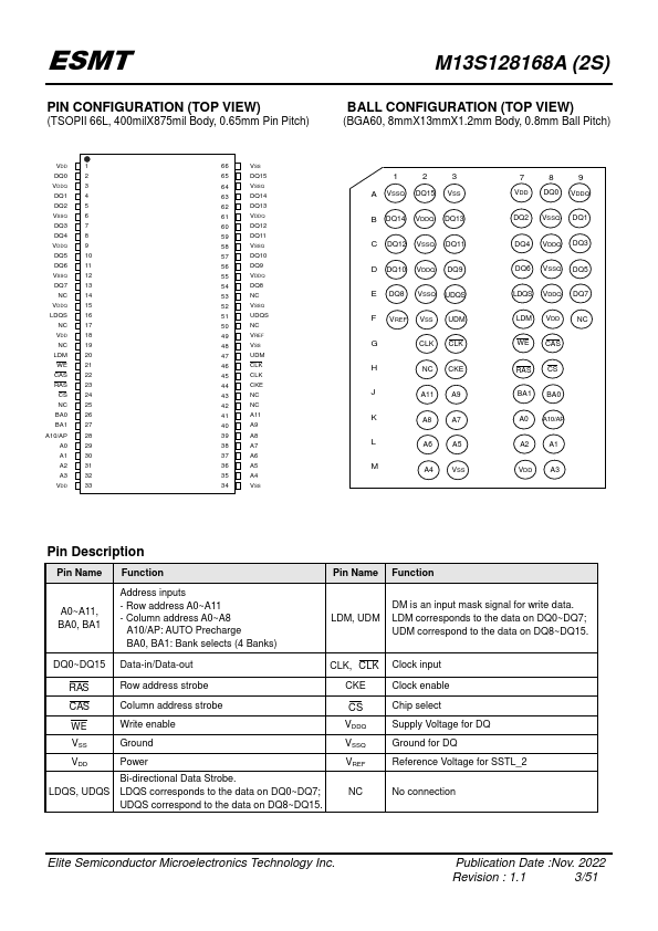
Pin Name Function Pin Name Function A0~A11, BA0, BA1 Address inputs - Row address A0~A11 - Column address A0~A8 A10/AP: AUTO Precharge BA0, BA1: Bank selects (4 Banks) DM is an input mask signal for write data.LDM, UDM LDM corresponds to the data on DQ0~DQ7; UDM correspond to the data on DQ8~DQ15. DQ0~DQ15 Data-in/Data-out CLK, CLK Clock input RAS Row address strobe CAS Column address strobe WE Write enable VSS Ground VDD LDQS, UDQS Power Bi-directional Data Strobe.LDQS corres
📁 M13S128168A Similar Datasheet