Datasheet Details
- Part number
- ICS9DB102
- Manufacturer
- Integrated Circuit Systems
- File Size
- 275.87 KB
- Datasheet
- ICS9DB102_IntegratedCircuitSystems.pdf
- Description
- 2 Output PCI Express Buffer
ICS9DB102 Description
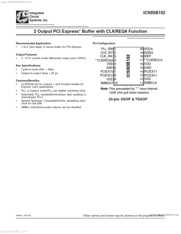
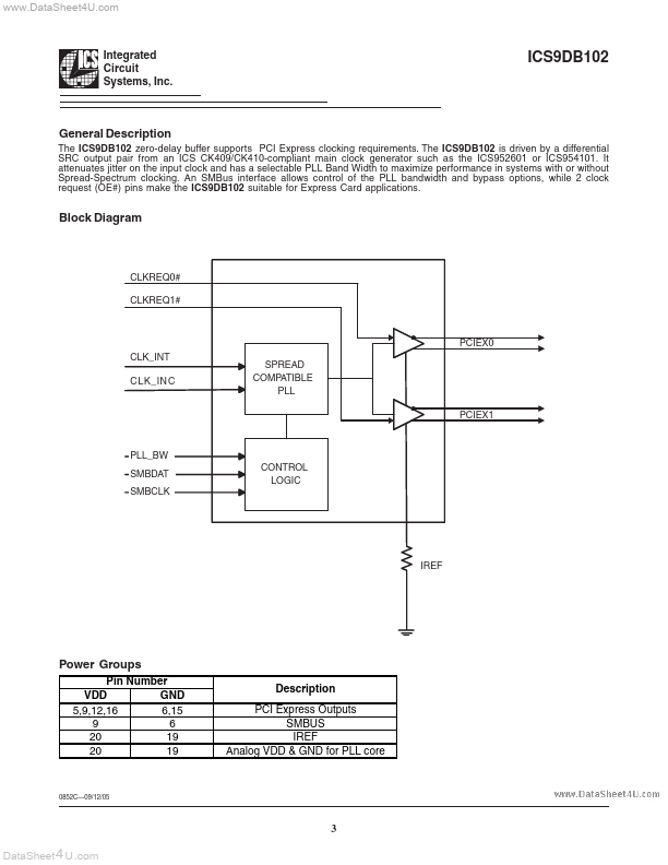
www.DataSheet4U.com Integrated Circuit Systems, Inc.ICS9DB102 2 Output PCI Express * Buffer with CLKREQ# Function Recommended Application: .
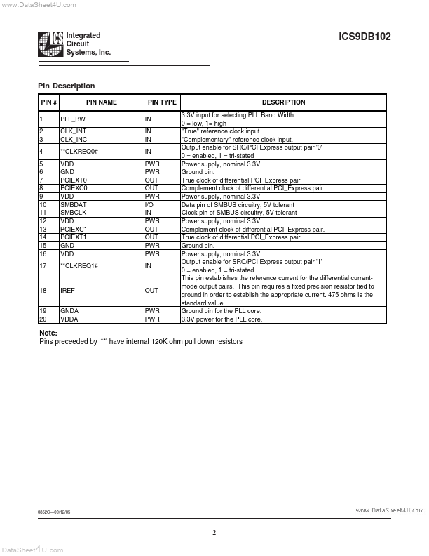
PIN # 1 2 3 4 5 6 7 8 9 10 11 12 13 14 15 16 17 PLL_BW CLK_INT CLK_INC.
CLKREQ0# VDD GND PCIEXT0 PCIEXC0 VDD SMBDAT SMBCLK VDD PCIEXC1 PCIEXT.
ICS9DB102 Features
* 2 - 0.7V current mode differential output pairs (HSCL) Key Specifications:
* Cycle-to-cycle jitter < 35ps
* Output-to-output skew < 25 ps Features/Benefits:
ICS9DB102 Applications
* PLL or bypass mode/PLL can dejitter incoming clock
* Selectable PLL bandwidth/minimizes jitter peaking in downstream PLL’s
* Spread Spectrum Compatible/tracks spreading input clock for low EMI
* SMBus Interface/unused outputs can be disabled Pin Configuration
PLL_B
📁 Related Datasheet
📌 All Tags
ICS9DB102 Stock/Price