Datasheet Details
| Part number | NCP51145 |
|---|---|
| Manufacturer | ON Semiconductor |
| File Size | 76.41 KB |
| Description | Termination Regulator |
| Datasheet |
 NCP51145 Datasheet NCP51145 Datasheet
|
|
|
| Part number | NCP51145 |
|---|---|
| Manufacturer | ON Semiconductor |
| File Size | 76.41 KB |
| Description | Termination Regulator |
| Datasheet |
NCP51145 Datasheet
|
|
|
|
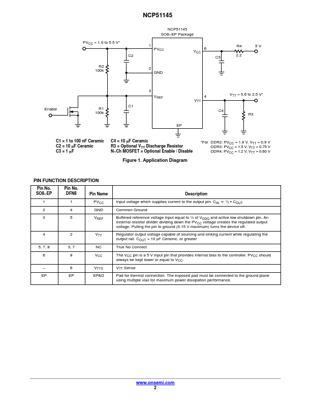
Pin No. EP Pin No.DFN8 Pin Name 1 1 PVCC 2 4 GND 3 5 VREF 4 2 VTT 5, 7, 8 6 3, 7 8 NC VCC 6 VTTS EP EP EPAD Description Input voltage which supplies current to the output pin.CIN ^ ½ S COUT Common Ground Buffered reference voltage input equal to ½ of VDDQ and active low shutdown pin.An external resistor divider dividing down the PVCC voltage creates the regulated output voltage.Pulling the pin to ground (0.15 V maximum) turns the device off.Regulator output
📁 Similar Datasheet