Datasheet Details
| Part number | NCP51198 |
|---|---|
| Manufacturer | ON Semiconductor |
| File Size | 217.03 KB |
| Description | 1.5A DDR Memory Termination Regulator |
| Datasheet |
 NCP51198 Datasheet NCP51198 Datasheet
|
|
|
| Part number | NCP51198 |
|---|---|
| Manufacturer | ON Semiconductor |
| File Size | 217.03 KB |
| Description | 1.5A DDR Memory Termination Regulator |
| Datasheet |
NCP51198 Datasheet
|
|
|
|
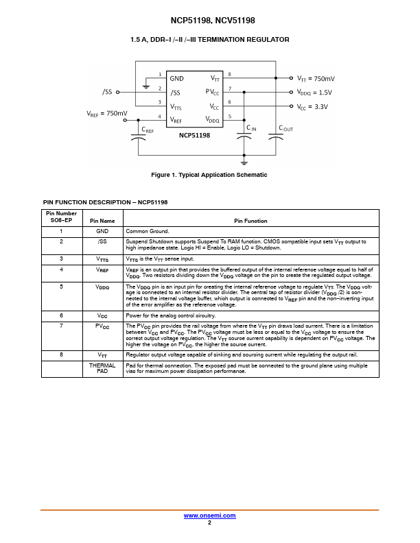
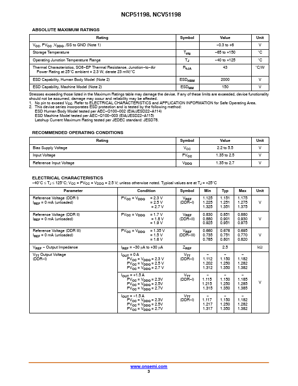
NCP51198 Pin Number SO8 EP Pin Name Pin Function 1 GND Common Ground.2 /SS Suspend Shutdown supports Suspend To RAM function.CMOS compatible input sets VTT output to high impedance state.Logic HI = Enable, Logic LO = Shutdown.3 VTTS VTTS is the VTT sense input.4 VREF VREF is an output pin that provides the buffered output of the internal reference voltage equal to half of VDDQ.Two resistors dividing down the VDDQ voltage on the pin to create the regulated
📁 Similar Datasheet