Datasheet Details
| Part number | NCP51199 |
|---|---|
| Manufacturer | ON Semiconductor |
| File Size | 67.39 KB |
| Description | Termination Regulator |
| Datasheet |
 NCP51199 Datasheet NCP51199 Datasheet
|
|
|
| Part number | NCP51199 |
|---|---|
| Manufacturer | ON Semiconductor |
| File Size | 67.39 KB |
| Description | Termination Regulator |
| Datasheet |
NCP51199 Datasheet
|
|
|
|
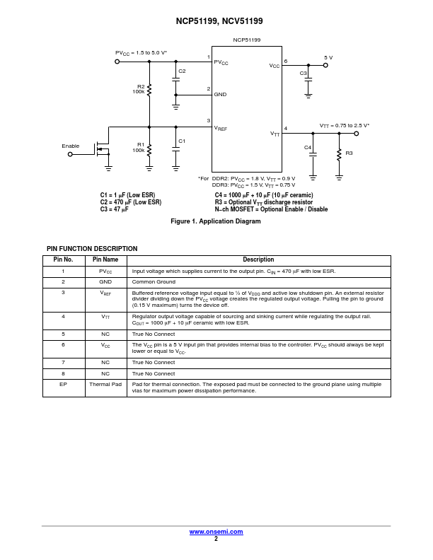
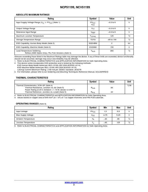
Pin No.
📁 Similar Datasheet