Datasheet Details
| Part number | HD74LVC1G17 |
|---|---|
| Manufacturer | Renesas Technology |
| File Size | 2.26 MB |
| Description | Schmitt-trigger Buffer |
| Datasheet |
 HD74LVC1G17 Datasheet HD74LVC1G17 Datasheet
|
|
|
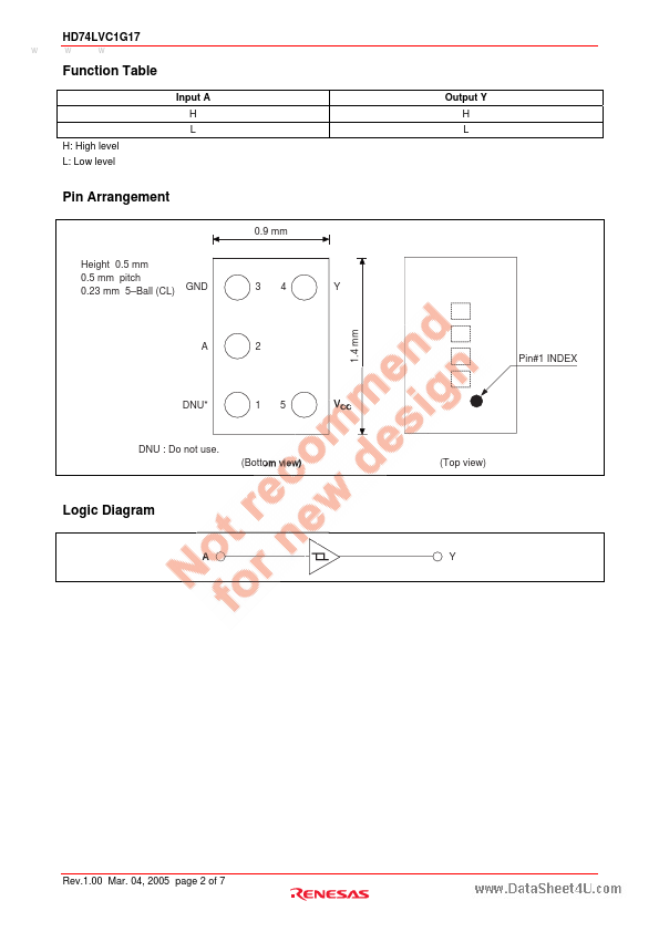
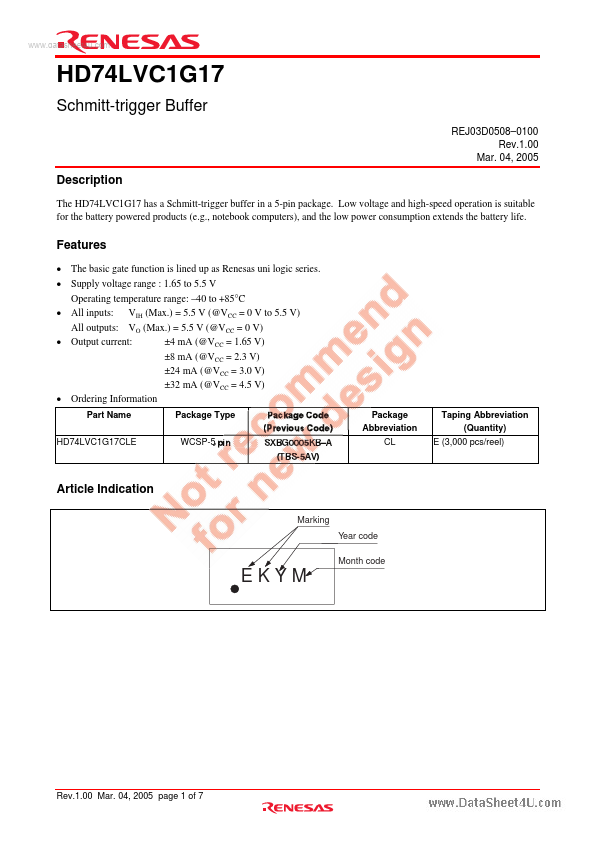
The HD74LVC1G17 has a Schmitt-trigger buffer in a 5-pin package.
Low voltage and high-speed operation is suitable for the battery powered products (e.g., notebook computers), and the low power consumption extends the battery life.
| Part number | HD74LVC1G17 |
|---|---|
| Manufacturer | Renesas Technology |
| File Size | 2.26 MB |
| Description | Schmitt-trigger Buffer |
| Datasheet |
HD74LVC1G17 Datasheet
|
|
|
|