Datasheet Details
| Part number | ICS9LPRS535 |
|---|---|
| Manufacturer | Renesas |
| File Size | 395.28 KB |
| Description | VREG |
| Datasheet |
 ICS9LPRS535 Datasheet ICS9LPRS535 Datasheet
|
|
|
| Part number | ICS9LPRS535 |
|---|---|
| Manufacturer | Renesas |
| File Size | 395.28 KB |
| Description | VREG |
| Datasheet |
ICS9LPRS535 Datasheet
|
|
|
|
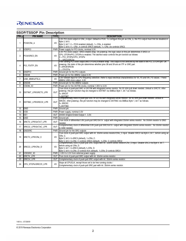
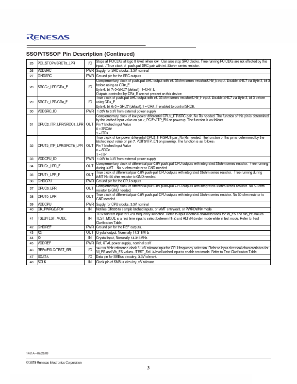
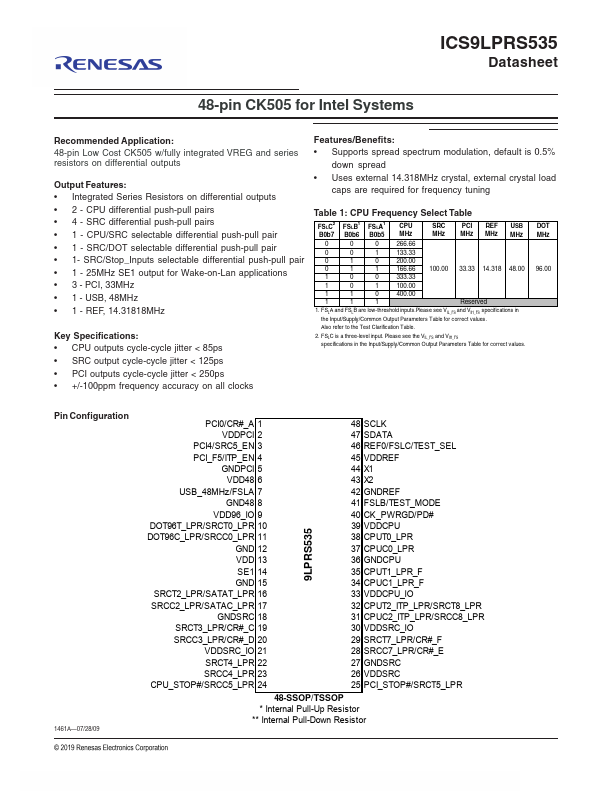
PIN # PIN NAME 1 PCI0/CR#_A 2 VDDPCI 3 PCI4/SRC5_EN 4 PCI_F5/ITP_EN 5 GNDPCI 6 VDD48 7 USB_48MHz/FSLA 8 GND48 9 VDD96_IO 10 DOT96T_LPR/SRCT0_LPR 11 DOT96C_LPR/SRCC0_LPR 12 GND TYPE DESCRIPTION 3.3V PCI clock output or CR#_A input.Default is PCI0. To configure this pin as CR#_A, the PCI output must first be disabled in I/O Byte 2, bit 0. Byte 5, bit 7: 0 = PCI0 enabled (default), 1= CR#_A enabled.Byte 5, bit 6: 0 = CR#_A controls SRC0 (default), 1= CR#_A# controls SRC2. PWR Power su
📁 Similar Datasheet