Datasheet4U Logo Datasheet4U.com

KM718V987 (KM736V887 / KM718V987) 256Kx36 & 512Kx18 Synchronous SRAM

📥 Download Datasheet  Datasheet Preview Page 1

Description

KM736V887 KM718V987 Document Title 256Kx36 & 512Kx18 Synchronous SRAM 256Kx36 & 512Kx18-Bit Synchronous Burst SRAM Revision History Rev.No.0.0 0..
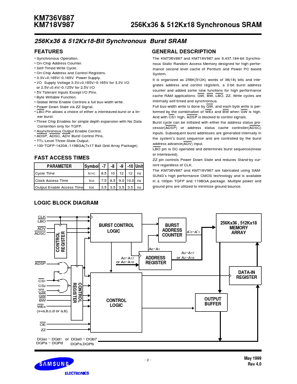
The KM736V887 and KM718V987 are 9,437,184-bit Synchronous Static Random Access Memory designed for high performance second level cache of Pentium and.

📥 Download Datasheet

Preview of KM718V987 PDF
datasheet Preview Page 2 datasheet Preview Page 3

Datasheet Specifications

Part number
KM718V987
Manufacturer
Samsung semiconductor
File Size
574.50 KB
Datasheet
KM718V987_Samsungsemiconductor.pdf
Description
(KM736V887 / KM718V987) 256Kx36 & 512Kx18 Synchronous SRAM

Features

* Synchronous Operation.
* On-Chip Address Counter.
* Self-Timed Write Cycle.
* On-Chip Address and Control Registers.
* 3.3V+0.165V/-0.165V Power Supply.
* I/O Supply Voltage 3.3V+0.165V/-0.165V for 3.3V I/O or 2.5V+0.4V/-0.125V for 2.5V I/O

Applications

* GW, BW, LBO, ZZ. Write cycles are internally self-timed and synchronous. Full bus-width write is done by GW, and each byte write is performed by the combination of WEx and BW when GW is high. And with CS1 high, ADSP is blocked to control signals. Burst cycle can be initiated with either the address

KM718V987 Distributors

📁 Related Datasheet

📌 All Tags

Samsung semiconductor KM718V987-like datasheet