Datasheet Details
| Part number | AOU413 |
|---|---|
| Manufacturer | Alpha & Omega Semiconductors |
| File Size | 103.34 KB |
| Description | P-Channel MOSFET |
| Download | AOU413 Download (PDF) |
|
|
| Part number | AOU413 |
|---|---|
| Manufacturer | Alpha & Omega Semiconductors |
| File Size | 103.34 KB |
| Description | P-Channel MOSFET |
| Download | AOU413 Download (PDF) |
|
|
|
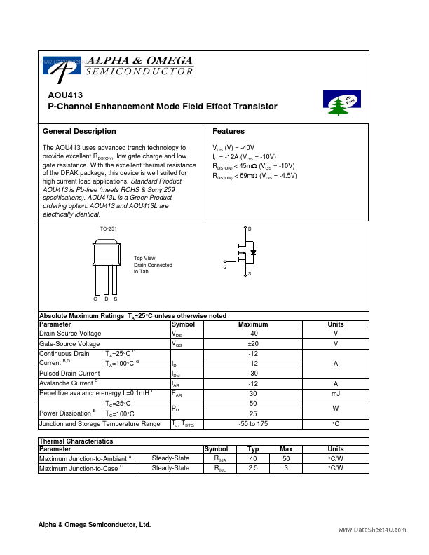
The AOU413 uses advanced trench technology to provide excellent RDS(ON), low gate charge and low gate resistance.
With the excellent thermal resistance of the DPAK package, this device is well suited for high current load applications.
Standard Product AOU413 is Pb-free (meets ROHS & Sony 259 specifications).
www.DataSheet4U.com AOU413 P-Channel Enhancement Mode Field Effect.
| Part Number | Description |
|---|---|
| AOU412 | N-Channel MOSFET |
| AOU414 | N-Channel MOSFET |
| AOU417 | P-Channel MOSFET |
| AOU400 | N-Channel MOSFET |
| AOU401 | P-Channel MOSFET |
| AOU402 | N-Channel MOSFET |
| AOU403 | P-Channel MOSFET |
| AOU404 | N-Channel MOSFET |
| AOU405 | P-Channel MOSFET |
| AOU408 | N-Channel MOSFET |