Datasheet Details
| Part number | AOU417 |
|---|---|
| Manufacturer | Alpha & Omega Semiconductors |
| File Size | 151.90 KB |
| Description | P-Channel MOSFET |
| Download | AOU417 Download (PDF) |
|
|
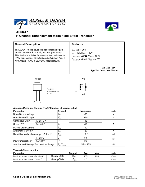
Overview: www.DataSheet4U.com AOU417 P-Channel Enhancement Mode Field Effect.
| Part number | AOU417 |
|---|---|
| Manufacturer | Alpha & Omega Semiconductors |
| File Size | 151.90 KB |
| Description | P-Channel MOSFET |
| Download | AOU417 Download (PDF) |
|
|
|
The AOU417 uses advanced trench technology to provide excellent RDS(ON), and low gate charge.
This device is suitable for use as a load switch or in PWM applications.
Standard product AOU417 is Pbfree (meets ROHS & Sony 259 specifications).
| Part Number | Description |
|---|---|
| AOU412 | N-Channel MOSFET |
| AOU413 | P-Channel MOSFET |
| AOU414 | N-Channel MOSFET |
| AOU400 | N-Channel MOSFET |
| AOU401 | P-Channel MOSFET |
| AOU402 | N-Channel MOSFET |
| AOU403 | P-Channel MOSFET |
| AOU404 | N-Channel MOSFET |
| AOU405 | P-Channel MOSFET |
| AOU408 | N-Channel MOSFET |