FEATURES
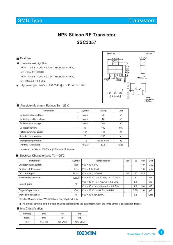
Low Noise and High Gain NF = 1.1 dB TYP., Ga = 7.5 dB TYP. @VCE = 10 V, IC = 7 mA, f = 1.0 GHz NF = 1.8 dB TYP., Ga = 9.0 dB TYP. @VCE = 10 V, IC = 40 mA, f = 1.0 GHz High power gain : MAG = 10 dB TYP. @ IC = 40 mA, f = 1 GHz ABSOLUTE MAXIMUM RATINGS
Ta = 25 Parameter Collector-base voltage Collector-emitter voltage Emitter-base voltage Collector current Total power dissipation Junction temperature Storage temperature Thermal Resistance * mounted on 16 cm X 0.7 mm(t) Ceramic Substrate 2 Symbol VCBO VCEO VEBO IC PT* Tj Tstg Rth(j-a)* Rating 20 12 3.0 100 1.2 150 -65 to +150 62.5 Unit V V V mA W /W ELECTRICAL CHARACTERISTICS
Ta = 25 Parameter Collector cutoff current Emitter cutoff current DC current gain Insertion Power Gain Noise Figure Output Capacitance Transition frequency *1 Pulse Measurement PW 350 ms, Duty Cycle Symbol ICBO IEBO hFE *1 |S21e|2 NF Cob fT 2% Testconditons VCB = 10V,IE=0 VEB = 1.0V,IC=0 VCE =10V,Ic=20mA VCE = 10 V, IC = 20 mA, f = 1.0 GHz VCE = 10 V, IC = 7...