FEATURES
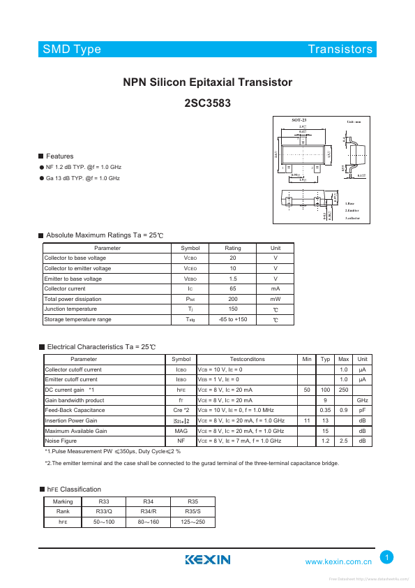
NF 1.2 dB TYP. @f = 1.0 GHz Ga 13 dB TYP. @f = 1.0 GHz +0.1 1.3-0.1 1 +0.1 0.95-0.1 +0.1 1.9-0.1 2 0.55 0.4 3 +0.05 0.1-0.01 +0.1 0.97-0.1 1.Base 2.Emitter 3.collector ABSOLUTE MAXIMUM RATINGS
Ta = 25 Parameter Collector to base voltage Collector to emitter voltage Emitter to base voltage Collector current Total power dissipation Junction temperature Storage temperature range Symbol VCBO VCEO VEBO IC Ptot Tj Tstg Rating 20 10 1.5 65 200 150 -65 to +150 Unit V V V mA mW ELECTRICAL CHARACTERISTICS
Ta = 25 Parameter Collector cutoff current Emitter cutoff current DC current gain *1 Gain bandwidth product Feed-Back Capacitance Insertion Power Gain Maximum Available Gain Noise Figure *1.Pulse Measurement PW Symbol ICBO IEBO hFE fT Cre *2 | MAG NF 350ìs, Duty Cycle 2 % Testconditons VCB = 10 V, IE = 0 VEB = 1 V, IE = 0 VCE = 8 V, IC = 20 mA VCE = 8 V, IC = 20 mA VCB = 10 V, IE = 0, f = 1.0 MHz VCE = 8 V, IC = 20 mA, f = 1.0 GHz VCE = 8 V, IC = 20 mA, f = 1.0 GHz VCE = 8 V, IE = 7 mA...