Datasheet4U Logo Datasheet4U.com

CY7C1372C - 512K x 36/1M x 18 Pipelined SRAM with NoBL Architecture

Datasheet Summary

Description

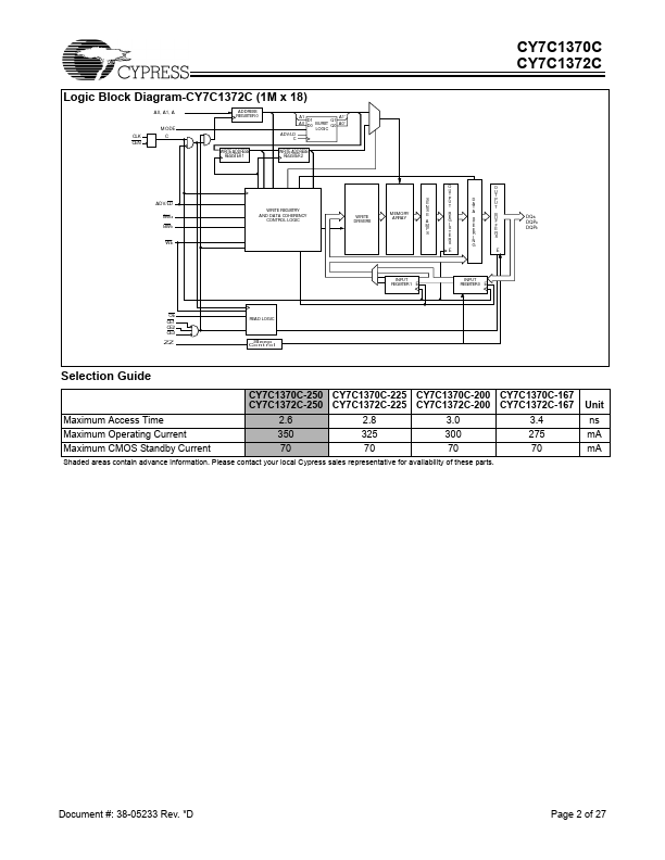
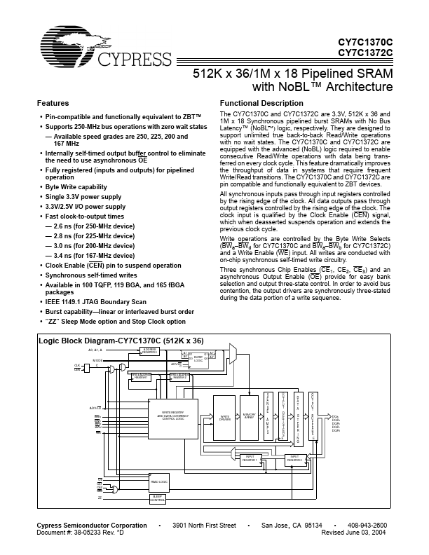
The CY7C1370C and CY7C1372C are 3.3V, 512K x 36 and 1M x 18 Synchronous pipelined burst SRAMs with No Bus Latency™ (NoBL) logic, respectively.

They are designed to support unlimited true back-to-back Read/Write operations with no wait states.

Features

  • Pin-compatible and functionally equivalent to ZBT™.
  • Supports 250-MHz bus operations with zero wait states.
  • Available speed grades are 250, 225, 200 and 167 MHz.
  • Internally self-timed output buffer control to eliminate the need to use asynchronous OE.
  • Fully registered (inputs and outputs) for pipelined operation.
  • Byte Write capability.
  • Single 3.3V power supply.
  • 3.3V/2.5V I/O power supply.
  • Fast clock-to-output times.

📥 Download Datasheet

Datasheet preview – CY7C1372C

Datasheet Details

Part number CY7C1372C
Manufacturer Cypress
File Size 704.25 KB
Description 512K x 36/1M x 18 Pipelined SRAM with NoBL Architecture
Datasheet download datasheet CY7C1372C Datasheet
Additional preview pages of the CY7C1372C datasheet.
Other Datasheets by Cypress

Full PDF Text Transcription

Click to expand full text
CY7C1370C CY7C1372C 512K x 36/1M x 18 Pipelined SRAM with NoBL™ Architecture Features • Pin-compatible and functionally equivalent to ZBT™ • Supports 250-MHz bus operations with zero wait states — Available speed grades are 250, 225, 200 and 167 MHz • Internally self-timed output buffer control to eliminate the need to use asynchronous OE • Fully registered (inputs and outputs) for pipelined operation • Byte Write capability • Single 3.3V power supply • 3.3V/2.5V I/O power supply • Fast clock-to-output times — 2.6 ns (for 250-MHz device) — 2.8 ns (for 225-MHz device) — 3.0 ns (for 200-MHz device) — 3.4 ns (for 167-MHz device) • Clock Enable (CEN) pin to suspend operation • Synchronous self-timed writes • Available in 100 TQFP, 119 BGA, and 165 fBGA packages • IEEE 1149.
Published: |