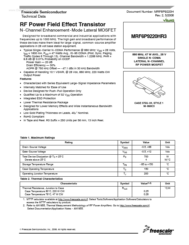
MRF6P9220HR3
Features
- Characterized with Series Equivalent Large
- Signal Impedance Parameters
- Internally Matched for Ease of Use
- Device Designed for Push
- Pull Operation Only
- Qualified Up to a Maximum of 32 VDD Operation
- Integrated ESD Protection
- Lower Thermal Resistance Package
- Designed for Lower Memory Effects and Wide Instantaneous Bandwidth Applications
- Low Gold Plating Thickness on Leads, 40μ″ Nominal.
- Ro HS pliant
- In Tape and Reel. R3 Suffix = 250 Units per 56 mm, 13 inch Reel.
880 MHz, 47 W AVG., 28 V SINGLE N
- CDMA LATERAL N
- CHANNEL RF POWER MOSFET
CASE 375G
- 04, STYLE 1 NI
- 860C3
Table 1. Maximum Ratings
Rating Drain- Source Voltage Gate- Source Voltage Total Device Dissipation @ TC = 25°C Derate above 25°C Storage Temperature Range Case Operating Temperature Operating Junction Temperature Symbol VDSS VGS PD Tstg TC TJ Value
- 0.5, +68
- 0.5, +12 700 4
- 65 to +150 150 200 Unit Vdc Vdc W W/°C °C °C °C
Table 2. Thermal Characteristics
Characterist...