Datasheet4U Logo Datasheet4U.com

MRFE6S9135HSR3 - N-Channel Enhancement-Mode Lateral MOSFETs

Download the MRFE6S9135HSR3 datasheet PDF. This datasheet also covers the MRFE6S9135HR3 variant, as both devices belong to the same n-channel enhancement-mode lateral mosfets family and are provided as variant models within a single manufacturer datasheet.

General Description

Part Number 2743019447 ATC100B390JT500XT 27291SL ATC100B2R0JT500XT EMVY250ADA330MF55G GRM55DR61H106KA88B ATC100B6R8JT500XT ATC100B4R7JT500XT EKME630ELL471MK25S CRCW12103R30FKEA CRCW12062201FKEA Manufacturer Fair- Rite ATC Johanson ATC Nippon Chemi - Con Murata ATC ATC United Chemi - Con Vishay Visha

Key Features

  • 100% PAR Tested for Guaranteed Output Power Capability.
  • Characterized with Series Equivalent Large - Signal Impedance Parameters.
  • Internally Matched for Ease of Use.
  • Qualified Up to a Maximum of 32 VDD Operation.
  • Integrated ESD Protection.
  • Optimized for Doherty.

📥 Download Datasheet

Note: The manufacturer provides a single datasheet file (MRFE6S9135HR3_FreescaleSemiconductor.pdf) that lists specifications for multiple related part numbers.

Full PDF Text Transcription (Reference)

The following content is an automatically extracted verbatim text from the original manufacturer datasheet and is provided for reference purposes only.

View original datasheet text
www.DataSheet4U.com 
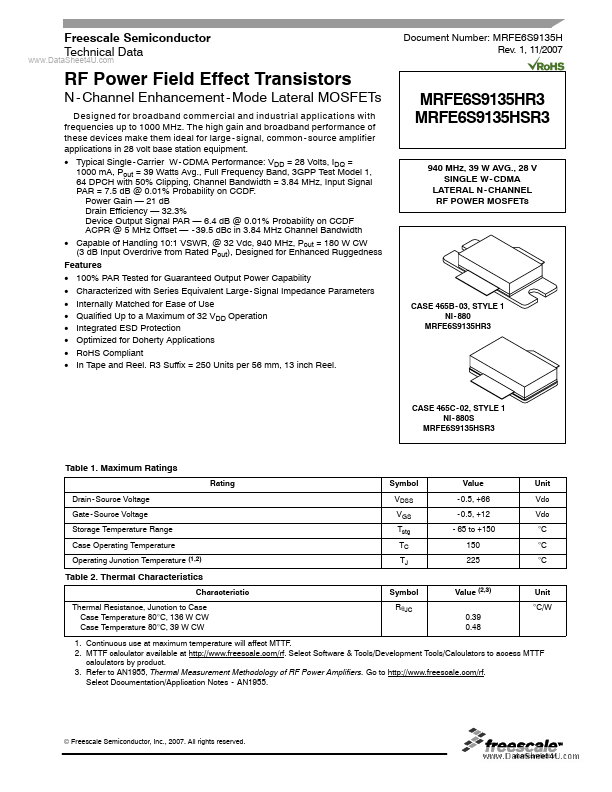
Freescale Semiconductor Technical Data Document Number: MRFE6S9135H Rev. 1, 11/2007 RF Power Field Effect Transistors N - Channel Enhancement - Mode Lateral MOSFETs Designed for broadband commercial and industrial applications with frequencies up to 1000 MHz. The high gain and broadband performance of these devices make them ideal for large - signal, common - source amplifier applications in 28 volt base station equipment. • Typical Single- Carrier W - CDMA Performance: VDD = 28 Volts, IDQ = 1000 mA, Pout = 39 Watts Avg., Full Frequency Band, 3GPP Test Model 1, 64 DPCH with 50% Clipping, Channel Bandwidth = 3.84 MHz, Input Signal PAR = 7.5 dB @ 0.01% Probability on CCDF. Power Gain — 21 dB Drain Efficiency — 32.3% Device Output Signal PAR — 6.4 dB @ 0.