STN442D
DESCRIPTION
STN442D is used trench technology to provide excellent RDS(on) and gate charge. Those devices are suitable for use as load switch or in PWM applications.
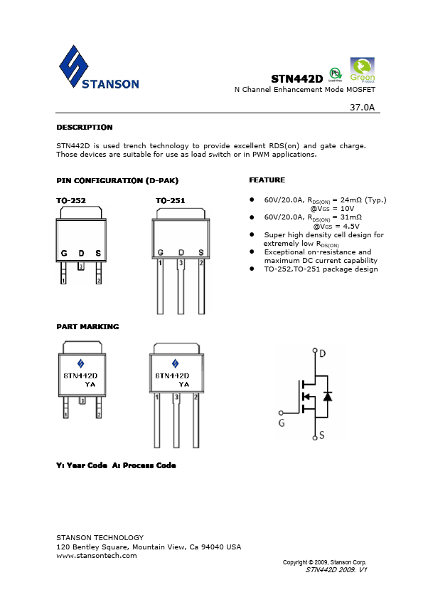
PIN CONFIGURATION (D-PAK)
TO-252
TO-251
FEATURE
- 60V/20.0A, RDS(ON) = 24mΩ (Typ.) @VGS = 10V
- 60V/20.0A, RDS(ON) = 31mΩ @VGS = 4.5V
- Super high density cell design for extremely low RDS(ON)
- Exceptional on-resistance and maximum DC current capability
- TO-252,TO-251 package design
PART MARKING
Y: Year Code A: Process Code
STANSON TECHNOLOGY 120 Bentley Square, Mountain View, Ca 94040 USA .stansontech.
Copyright © 2009, Stanson Corp.
STN442D 2009. V1
N Channel Enhancement Mode MOSFET
37.0A
ABSOULTE MAXIMUM RATINGS (Ta = 25℃ Unless otherwise noted )
Parameter
Symbol
Drain-Source Voltage
VDSS
Gate-Source Voltage
Continuous Drain Current (TJ=150℃)
TA=25℃ TA=70℃
Pulsed Drain Current
VGSS ID
Continuous Source Current (Diode Conduction)
Power Dissipation
TA=25℃ TA=70℃
Operation Junction...