High Density Cell Design for Ultra Low On-resistance
Ordering Information
Block Diagram
Part No. Package
Packing
TSM3911DCX6 RF
SOT-26
3kpcs / 7” Reel
TSM3911DCX6 RFG
SOT-26
3kpcs / 7” Reel
Note: “G” denotes for Halogen- and Antimony-free as those which contain.
The following content is an automatically extracted verbatim text
from the original manufacturer datasheet and is provided for reference purposes only.
View original datasheet text
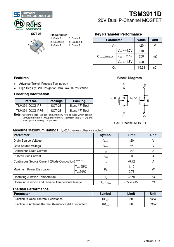
TSM3911D
20V Dual P-Channel MOSFET
SOT-26
Pin Definition:
1. Gate 1
6. Drain 1
2. Source 2 5. Source 1
3. Gate 2
4. Drain 2
Key Parameter Performance
Parameter
Value
VDS VGS = -4.5V
RDS(on) (max) VGS = -2.5V VGS = -1.8V
-20 140 200 300
Qg 15.23
Unit
V
mΩ
nC
Features
● Advance Trench Process Technology ● High Density Cell Design for Ultra Low On-resistance
Ordering Information
Block Diagram
Part No.