Datasheet4U Logo Datasheet4U.com

CY7C1217F - 1-Mbit (32K x 36) Flow-Through Sync SRAM

Datasheet Summary

Description

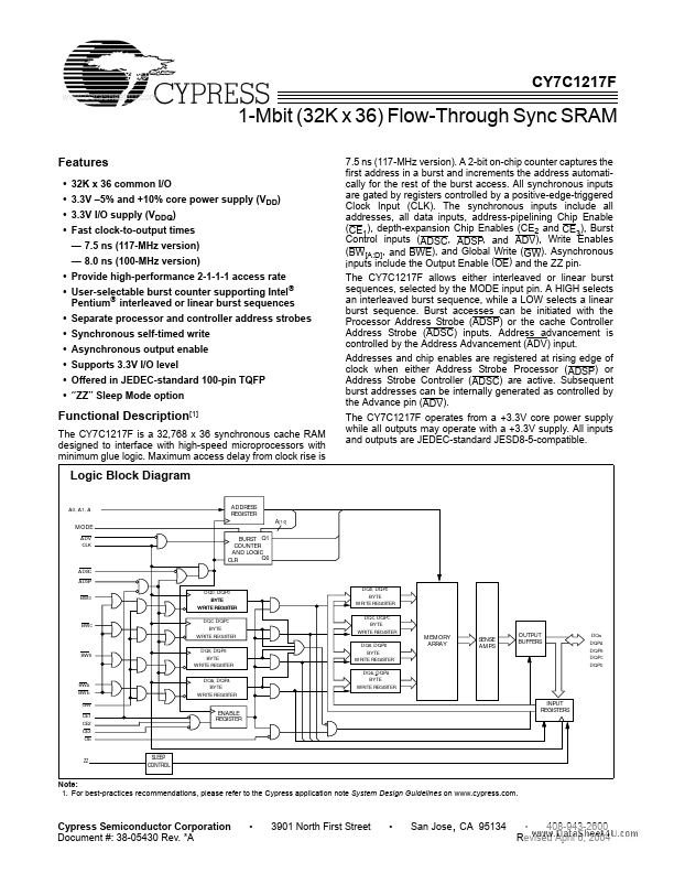
The CY7C1217F is a 32,768 x 36 synchronous cache RAM designed to interface with high-speed microprocessors with minimum glue logic.

Features

  • 32K x 36 common I/O.
  • 3.3V.
  • 5% and +10% core power supply (VDD).
  • 3.3V I/O supply (VDDQ).
  • Fast clock-to-output times.
  • 7.5 ns (117-MHz version).
  • 8.0 ns (100-MHz version).
  • Provide high-performance 2-1-1-1 access rate.
  • User-selectable burst counter supporting Pentium interleaved or linear burst sequences.
  • Separate processor and controller address strobes.
  • Synchronous self-timed write.
  • Asynchro.

📥 Download Datasheet

Datasheet preview – CY7C1217F

Datasheet Details

Part number CY7C1217F
Manufacturer Cypress Semiconductor
File Size 362.82 KB
Description 1-Mbit (32K x 36) Flow-Through Sync SRAM
Datasheet download datasheet CY7C1217F Datasheet
Additional preview pages of the CY7C1217F datasheet.
Other Datasheets by Cypress Semiconductor

Full PDF Text Transcription

Click to expand full text
CY7C1217F www.DataSheet4U.com 1-Mbit (32K x 36) Flow-Through Sync SRAM Features • 32K x 36 common I/O • 3.3V –5% and +10% core power supply (VDD) • 3.3V I/O supply (VDDQ) • Fast clock-to-output times — 7.5 ns (117-MHz version) — 8.0 ns (100-MHz version) • Provide high-performance 2-1-1-1 access rate • User-selectable burst counter supporting Pentium interleaved or linear burst sequences • Separate processor and controller address strobes • Synchronous self-timed write • Asynchronous output enable • Supports 3.3V I/O level • Offered in JEDEC-standard 100-pin TQFP • “ZZ” Sleep Mode option Intel 7.5 ns (117-MHz version). A 2-bit on-chip counter captures the first address in a burst and increments the address automatically for the rest of the burst access.
Published: |