Click to expand full text
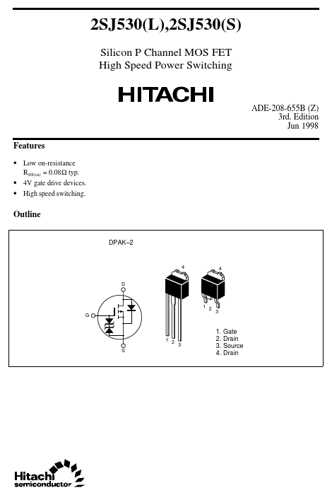
2SJ530(L),2SJ530(S)
Silicon P Channel MOS FET High Speed Power Switching
ADE-208-655B (Z) 3rd. Edition Jun 1998 Features
• Low on-resistance R DS(on) = 0.08 Ω typ. • 4V gate drive devices. • High speed switching.
Outline
DPAK–2
4 D
4
1 2 G
3
1 2 S
3
1. Gate 2. Drain 3. Source 4. Drain
2SJ530(L),2SJ530(S)
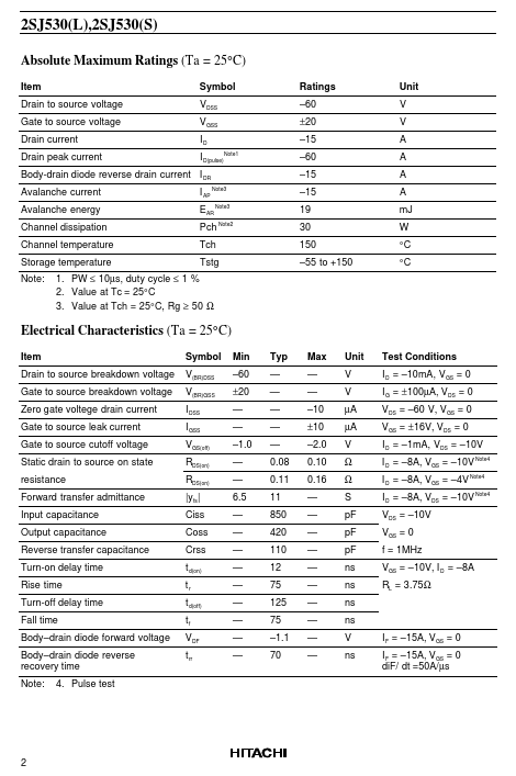
Absolute Maximum Ratings (Ta = 25°C)
Item Drain to source voltage Gate to source voltage Drain current Drain peak current Symbol VDSS VGSS ID I D(pulse)
Note1
Ratings –60 ±20 –15 –60 –15
Unit V V A A A A mJ W °C °C
Body-drain diode reverse drain current I DR Avalanche current Avalanche energy Channel dissipation Channel temperature Storage temperature Note: I AP
Note3 Note3 Note2
–15 19 30 150 –55 to +150
EAR
Pch Tch
Tstg
1. PW ≤ 10µs, duty cycle ≤ 1 % 2.
 2SJ530L Datasheet