Description
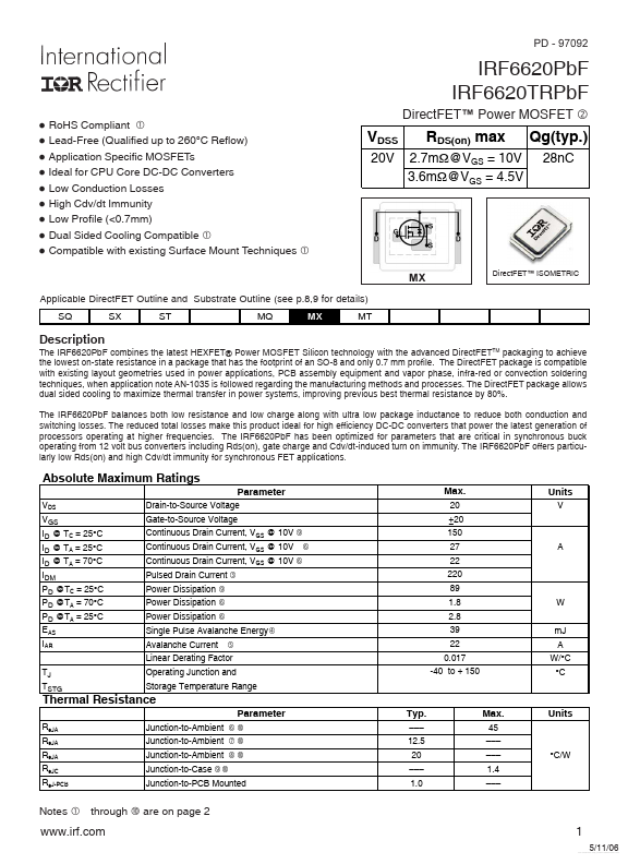
The IRF6620PbF combines the latest HEXFET® Power MOSFET Silicon technology with the advanced DirectFETTM packaging to achieve the lowest on-state resistance in a package that has the footprint of an SO-8 and only 0.7 mm profile.
Features
- + V - DD
A
D. U. T VGS Pulse Width < 1µs Duty Factor < 0.1%
0.01Ω
Fig 13a. Unclamped Inductive Test Circuit
V(BR)DSS tp
Fig 14a. Switching Time Test Circuit
90%
VDS
10%
VGS
I AS
td(on)
tr
td(off)
tf
Fig 13b. Unclamped Inductive Waveforms
Fig 14b. Switching Time Waveforms
Id Vds Vgs
L
0
DUT 1K
VCC
Vgs(th)
Qgs1 Qgs2
Qgd
Qgodr
Fig 15a. Gate Charge Test Circuit
Fig 15b. Gate Charge Waveform
www. irf. com
5
Free Datasheet http://www. Datasheet4U. com
IRF6620PbF
D. U. T
Driver Gate Dr.


