Datasheet Details
| Part number | MC100ES6130 |
|---|---|
| Manufacturer | Motorola |
| File Size | 342.63 KB |
| Description | 2.5/3.3V 1:4 PECL Clock Driver |
| Datasheet |
 MC100ES6130 Datasheet MC100ES6130 Datasheet
|
|
|
| Part number | MC100ES6130 |
|---|---|
| Manufacturer | Motorola |
| File Size | 342.63 KB |
| Description | 2.5/3.3V 1:4 PECL Clock Driver |
| Datasheet |
MC100ES6130 Datasheet
|
|
|
|
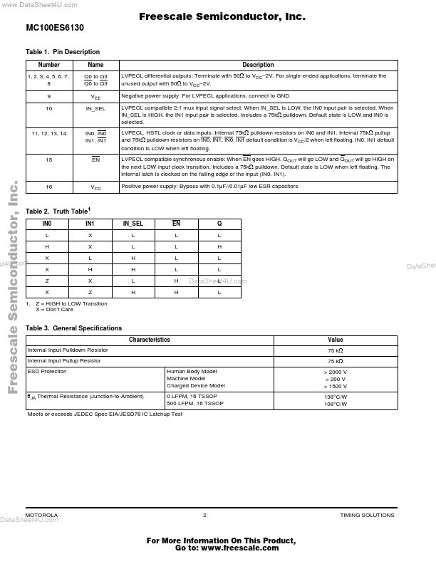
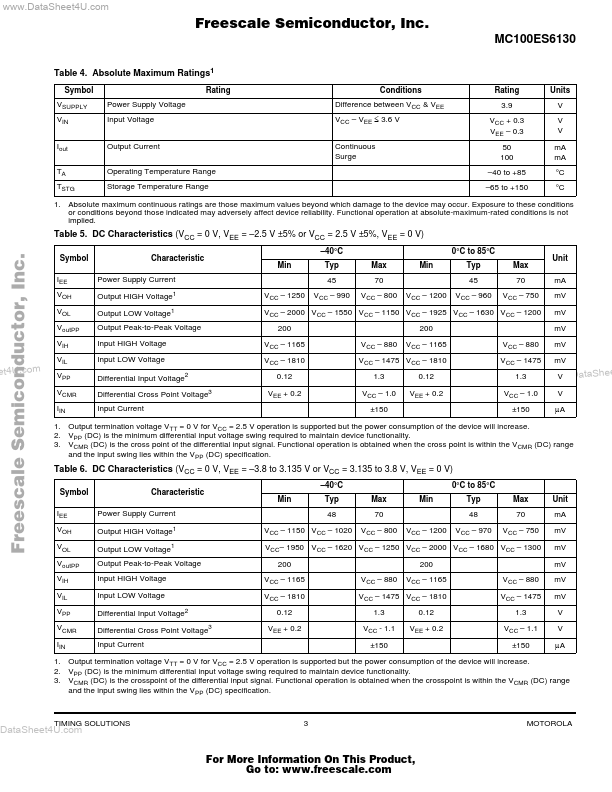
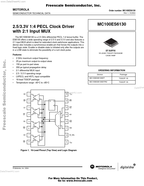
Number 1, 2, 3, 4, 5, 6, 7, 8 9 10 Name Q0 to Q3 Q0 to Q3 VEE IN_SEL Description LVPECL differential outputs: Terminate with 50Ω to VCC 2V. 2V.
📁 Similar Datasheet