Datasheet Details
- Part number
- ICS9DB102
- Manufacturer
- Renesas ↗
- File Size
- 262.60 KB
- Datasheet
- ICS9DB102-Renesas.pdf
- Description
- Two Output Differential Buffer
ICS9DB102 Description
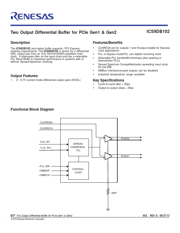
Two Output Differential Buffer for PCIe Gen1 & Gen2 DATASHEET ICS9DB102 .
The ICS9DB102 zero-delay buffer supports PCI Express clocking requirements.
ICS9DB102 Features
* 2 - 0.7V current mode differential output pairs (HCSL)
Features/Benefits
ICS9DB102 Applications
* PLL or bypass mode/PLL can dejitter incoming clock
* Selectable PLL bandwidth/minimizes jitter peaking in
downstream PLL’s
* Spread Spectrum Compatible/tracks spreading input clock
for low EMI
* SMBus Interface/unused outputs can be disabled
* Industrial tem
📁 Related Datasheet
📌 All Tags
ICS9DB102 Stock/Price