Click to expand full text
UMW FDN302P
P-ChanneI MOSFET
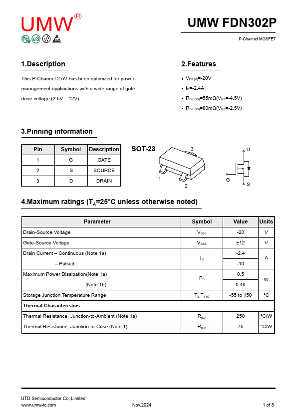
1.Description
This P-Channel 2.5V has been optimized for power management applications with a wide range of gate drive voltage (2.5V – 12V)
2.Features
VDS (V)=-20V ID=-2.4A RDS(ON)=55mΩ(VGS=-4.5V) RDS(ON)=80mΩ(VGS=-2.5V)
3.Pinning information
Pin
Symbol Description SOT-23
3
1
G
GATE
2
S
SOURCE
3
D
DRAIN
1 2
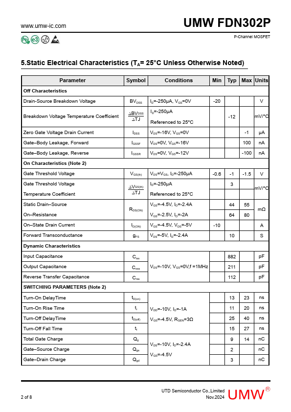
4.Maximum ratings (TA=25°C unless otherwise noted)
Parameter Drain-Source Voltage Gate-Source Voltage Drain Current – Continuous (Note 1a)
– Pulsed Maximum Power Dissipation(Note 1a)
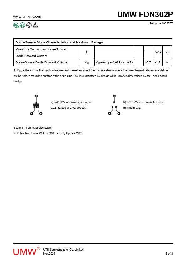
(Note 1b) Storage Junction Temperature Range Thermal Characteristics Thermal Resistance, Junction-to-Ambient (Note 1a) Thermal Resistance, Junction-to-Case (Note 1)
Symbol VDSS VGSS ID
PD TJ, TSTG
RθJA RθJC
D G
S
Value -20 ±12 -2.4 -10 0.5 0.
 FDN302P Datasheet