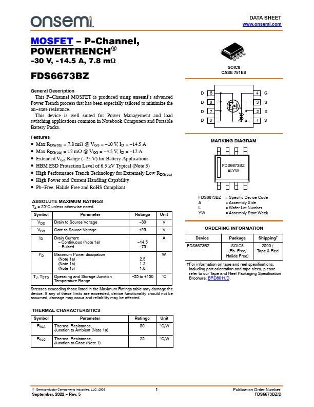
FDS6673BZ
Overview
This P-Channel MOSFET is produced using onsemi’s advanced Power Trench process that has been especially tailored to minimize the on-state resistance. This device is well suited for Power Management and load switching applications common in Notebook Computers and Portable Battery Packs.
- Max RDS(on) = 7.8 mW @ VGS = -10 V, ID = -14.5 A
- Max RDS(on) = 12 mW @ VGS = -4.5 V, ID = -12 A
- Extended VGS Range (-25 V) for Battery Applications
- HBM ESD Protection Level of 6.5 kV Typical (Note 3)
- High Performance Trench Technology for Extremely Low RDS(on)
- High Power and Current Handling Capability
- Pb-Free, Halide Free and RoHS Compliant