2SD2051
Key Features
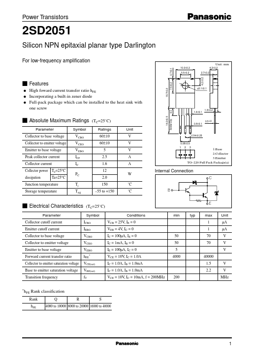
- 0 High foward current transfer ratio hFE Incorporating a built-in zener diode Full-pack package which can be installed to the heat sink with one screw (TC=25˚C) Ratings 60±10 60±10 5 2.5 1.6 12 2.0 150 -55 to +150 Unit V V V A A W ˚C ˚C
- 7±0.3 φ3.1±0.1
- 4±0.1
- 3±0.2 Solder Dip s Absolute Maximum Ratings Parameter Collector to base voltage Collector to emitter voltage Emitter to base voltage Peak collector current Collector current Collector power TC=25°C dissipation Ta=25°C Junction temperature Storage temperature Symbol VCBO VCEO VEBO ICP IC PC Tj Tstg
- 0±0.5
- 8±0.1
- 5 -0.1 +0.2
- 54±0.25 5.08±0.5 1 2 1:Base 2:Collector 3:Emitter TO-220 Full Pack Package(a) 3 Internal Connection C B s Electrical Characteristics Parameter Collector cutoff current Emitter cutoff current Collector to base voltage Collector to emitter voltage Emitter to base voltage Forward current transfer ratio Collector to emitter saturation voltage Base to emitter saturation voltage Transition frequency (TC=25˚C) Symbol ICBO IEBO VCBO VCEO VEBO hFE * E Conditions VCB = 25V, IE = 0 VEB = 4V, IC = 0 IC = 100µA, IE = 0 IC = 1mA, IB = 0 IE = 100µA, IC = 0 VCE = 10V, IC = 1.0A IC = 1.0A, IB = 1.0mA IC = 1.0A, IB = 1.0mA VCE = 10V, IC = 10mA, f = 200MHz min typ max 1 1 Unit µA µA V V V