• Part: NDP6030PL
  • Description: P-Channel Logic Level Enhancement Mode Field Effect Transistor
  • Category: Transistor
  • Manufacturer: Fairchild Semiconductor
  • Size: 56.60 KB
Download NDP6030PL Datasheet PDF
Fairchild Semiconductor
NDP6030PL
NDP6030PL is P-Channel Logic Level Enhancement Mode Field Effect Transistor manufactured by Fairchild Semiconductor.
Description These P-Channel logic level enhancement mode power field effect transistors are produced using Fairchild's proprietary, high cell density, DMOS technology. This very high density process is especially tailored to minimize on-state resistance. These devices are particularly suited for low voltage applications such as DC/DC converters and high efficiency switching circuits where fast switching, low in-line power loss, and resistance to transients are needed. Features -30 A, -30 V. RDS(ON) = 0.042 Ω @ VGS= -4.5 V RDS(ON) = 0.025 Ω @ VGS= -10 V. Critical DC electrical parameters specified at elevated temperature. Rugged internal source-drain diode can eliminate the need for an external Zener diode transient suppressor. High density cell design for extremely low RDS(ON). 175°C maximum junction temperature rating
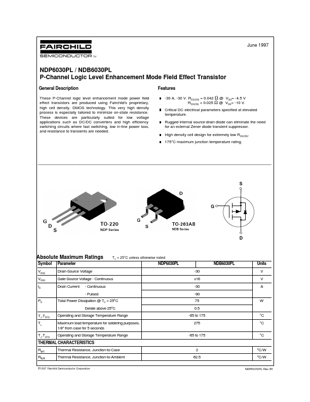
. Absolute Maximum Ratings Symbol VDSS VGSS ID PD Parameter Drain-Source Voltage T C = 25°C unless otherwise noted NDP6030PL -30 ±16 -30 -90 75 0.5 -65 to 175 275 -65 to 175 NDB6030PL Units V V A Gate-Source Voltage - Continuous Drain Current - Continuous - Pulsed Total Power Dissipation @ TC = 25°C Derate above 25°C TJ,TSTG TL TJ,TSTG RθJC RθJA Operating and Storage Temperature Range Maximum lead temperature for soldering purposes, 1/8" from case for 5 seconds Operating and Storage Temperature Range °C °C °C THERMAL CHARACTERISTICS Thermal Resistance, Junction-to-Case Thermal Resistance, Junction-to-Ambient 2 62.5 °C/W °C/W NDP6030PL Rev.B1 © 1997 Fairchild Semiconductor Corporation Electrical Characteristics (TC = 25°C unless otherwise noted) Symbol Parameter Conditions Min Typ Max Unit OFF CHARACTERISTICS BVDSS Drain-Source Breakdown Voltage Breakdown Voltage Temp. Coefficient Zero Gate Voltage Drain Current VGS = 0 V, ID = -250 µA ID = -250 µA, Referenced to 25 C VDS = -24 V, VGS = 0 V TJ = 125°C IGSSF IGSSR Gate - Body Leakage, Forward Gate...