FDN358P
FDN358P is P-Channel MOSFET manufactured by Fairchild Semiconductor.
Description
Super SOTTM-3 P-Channel logic level enhancement mode power field effect transistors are produced using Fairchild's proprietary, high cell density, DMOS technology. This very high density process is especially tailored to minimize on-state resistance. These devices are particularly suited for low voltage applications in notebook puters, portable phones, PCMCIA cards, and other battery powered circuits where fast switching, and low in-line power loss are needed in a very small outline surface mount package.
Features
-1.5 A, -30 V, RDS(ON) = 0.125 Ω @ VGS = -10 V RDS(ON) = 0.20 Ω @ VGS =
- 4.5 V. High power version of industry SOT-23 package: identical pin out to SOT-23; 30% higher power handling capability. High density cell design for extremely low RDS(ON). Exceptional on-resistance and maximum DC current capability.
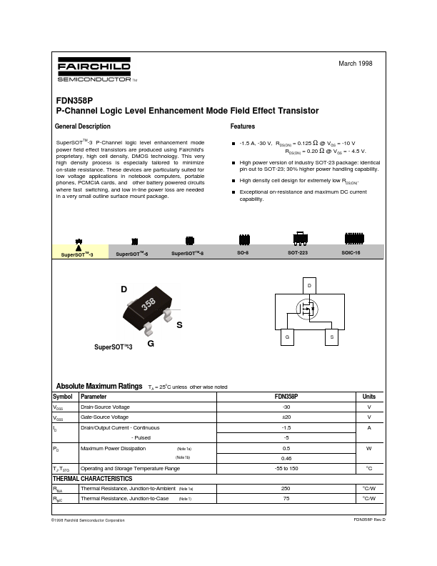
Super SOTTM-3
Super SOTTM-6
Super SOTTM-8
SO-8
SOT-223
SOIC-16
8 35
Super SOT -3
Absolute Maximum Ratings
Symbol VDSS VGSS ID PD TJ,TSTG RθJA RθJC Parameter Drain-Source Voltage Gate-Source Voltage
TA = 25o C unless other wise noted FDN358P -30 ±20 -1.5 -5
(Note 1a) (Note 1b)
Units V V A
Drain/Output Current
- Continuous
- Pulsed Maximum Power Dissipation
0.5 0.46 -55 to 150
Operating and Storage Temperature Range
°C
THERMAL CHARACTERISTICS Thermal Resistance, Junction-to-Ambient Thermal Resistance, Junction-to-Case
(Note 1a) (Note 1)
250 75
°C/W °C/W
© 1998 Fairchild Semiconductor Corporation
FDN358P Rev.D
Electrical Characteristics (TA = 25 OC unless otherwise noted )
Symbol Parameter Conditions Min Typ Max Units OFF CHARACTERISTICS BVDSS Drain-Source Breakdown Voltage Breakdown Voltage Temp. Coefficient Zero Gate Voltage Drain Current VGS = 0 V, ID = -250 µA ID = -250 µA, Referenced to 25 o C VDS = -24 V, VGS = 0 V TJ = 55°C IGSSF IGSSR VGS(th) Gate
- Body Leakage, Forward Gate
- Body Leakage,...