NXP Semiconductors BFG10
The BFG10 is capable of withstanding a load mismatch corresponding to VSWR = 8 : 1 through all phases, at rated output power under pulsed conditions up to a supply voltage of 7 V, f = 1.9 GHz and a duty cycle of 1 : 8. 1995 Aug 31 4 Philips Semiconductors Product specification NPN 2 GHz RF power transistor SPICE parameters for the BFG10 crystal SEQUENCE No.| Part No. | BFG10 |
|---|---|
| Datasheet | BFG10 Download |
| Manufacturer |  NXP Semiconductors |
| Description | NPN 2 GHz RF power transistor |
| Buy | Stock & Price |
FEATURES
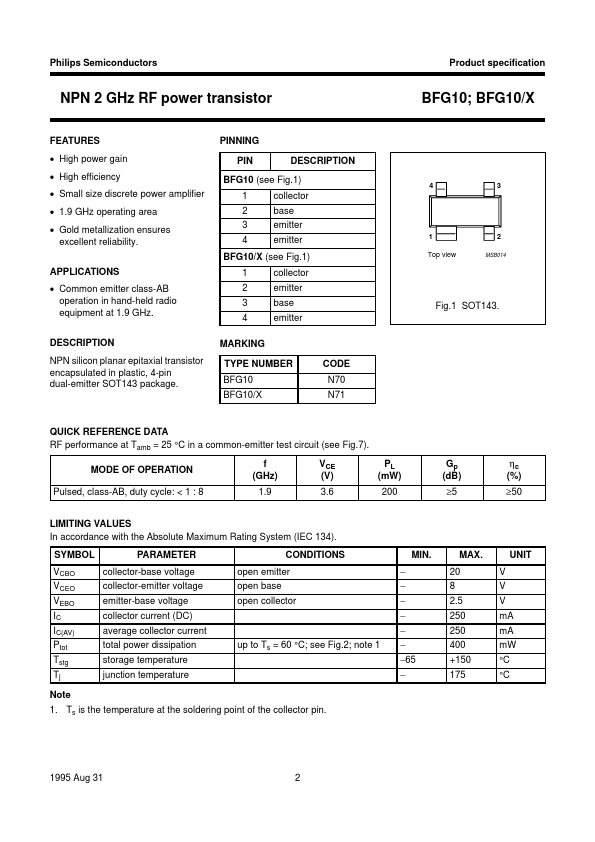
● High power gain● High efficiency
● Small size discrete power amplifier
● 1.9 GHz operating area
● Gold metallization ensures excellent reliability.
APPLICATIONS
● Common emitter class-AB operation in hand-held radio equipment at 1.9 GHz.DESCRIPTION
NPN silicon planar epitaxial transistor encapsulated in plastic, 4-pin dual-emitter SOT143 package. PINNING PINDESCRIPTION
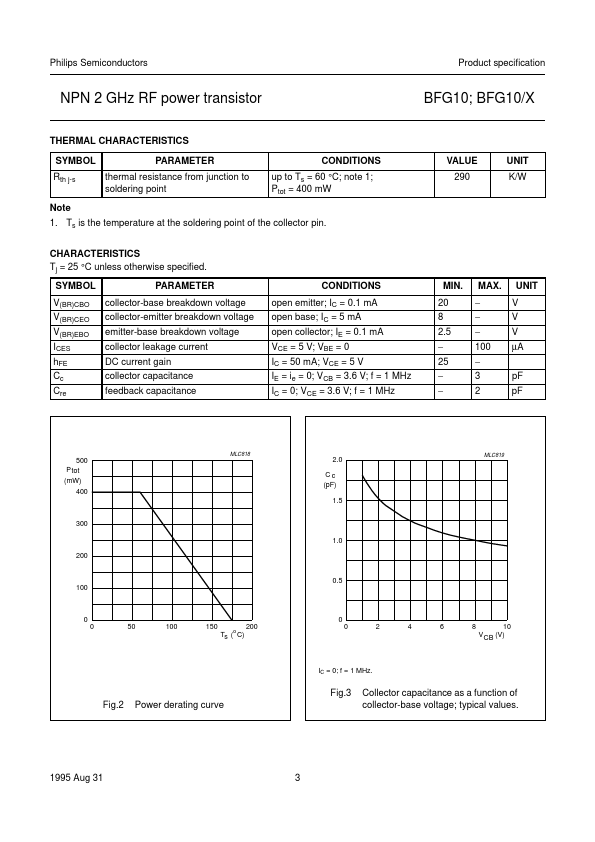
BFG10; BFG10/X BFG10 (see Fig.1) 1 2 3 4 collector base emitter emitter handbook, 2 columns 4 3 1 Top view 2 MSB014 BFG10/X (see Fig.1) 1 2 3 4 MARKING TYPE NUMBER BFG10 BFG10/X CODE N70 N71 collector emitter base emitter Fig.1 SOT143. QUICK REFERENCE DATA RF performance at Tamb = 25 °C in a common-emitter test circuit (see Fig.7). MODE OF OPERATION Pulsed, class-AB, duty cycle: < 1 : 8 f (GHz) 1.9 VCE (V) 3.6 PL (mW) 200 Gp (dB) ≥5 ηc (%) ≥50 LIMITING VALUES In accordance with the Absolute Maximum Rating System (IEC 134). SYMBOL VCBO VCEO VEBO IC IC(AV) Ptot Tstg Tj Note 1. Ts is the temperature at the soldering point of the collector pin.