NXP Semiconductors BFG10X
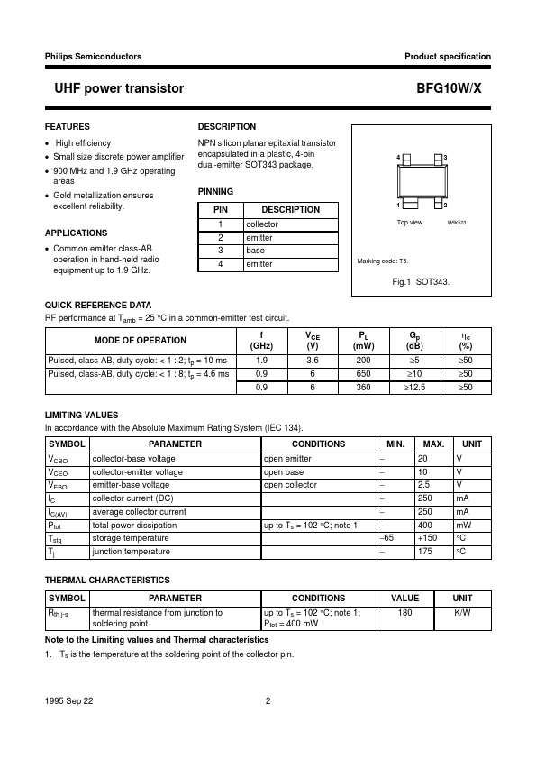
The BFG10W/X is capable of withstanding a load mismatch corresponding to VSWR = 6 : 1 through all phases under pulsed conditions up to a supply voltage of 8.6 V under the conditions: 900 MHz; 650 mW; tp = 4.6 ms; duty cycle of 1 : 8 and up to a supply voltage of 5.5 V under the conditions: 1.9 GHz; 200 mW; tp = 10 ms; duty cycle of 1 : 2.| Part No. | BFG10X |
|---|---|
| Datasheet | BFG10X Download |
| Manufacturer |  NXP Semiconductors |
| Description | UHF power transistor |
| Buy | Stock & Price |
FEATURES
● High efficiency● Small size discrete power amplifier
● 900 MHz and 1.9 GHz operating areas
● Gold metallization ensures excellent reliability.
APPLICATIONS
● Common emitter class-AB operation in hand-held radio equipment up to 1.9 GHz.DESCRIPTION
NPN silicon planar epitaxial transistor encapsulated in a plastic, 4-pin dual-emitter SOT343 package. PINNING PIN 1 2 3 4DESCRIPTION
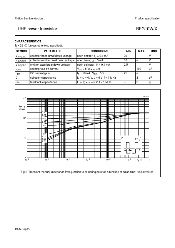
collector emitter base emitter Marking code: T5. 1 BFG10W/X fpage 4 3 2 MBK523 Top view Fig.1 SOT343. QUICK REFERENCE DATA RF performance at Tamb = 25 °C in a common-emitter test circuit. MODE OF OPERATION Pulsed, class-AB, duty cycle: < 1 : 2; tp = 10 ms Pulsed, class-AB, duty cycle: < 1 : 8; tp = 4.6 ms f (GHz) 1.9 0.9 0.9 LIMITING VALUES In accordance with the Absolute Maximum Rating System (IEC 134). SYMBOL VCBO VCEO VEBO IC IC(AV) Ptot Tstg Tj PARAMETER collector-base voltage collector-emitter voltage emitter-base voltage collector current (DC) average collector current total power dissipation storage temperature junction temperature up to Ts = 102 °C; note 1 CONDITIONS open emitter open base open collector − − − − − − −65 − MIN.