Datasheet Details
| Part number | AO6401 |
|---|---|
| Manufacturer | Alpha & Omega Semiconductors |
| File Size | 537.30 KB |
| Description | 30V P-Channel MOSFET |
| Download | AO6401 Download (PDF) |
|
|
| Part number | AO6401 |
|---|---|
| Manufacturer | Alpha & Omega Semiconductors |
| File Size | 537.30 KB |
| Description | 30V P-Channel MOSFET |
| Download | AO6401 Download (PDF) |
|
|
|
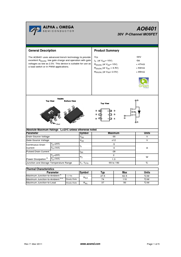
Product Summary The AO6401 uses advanced trench technology to provide excellent RDS(ON), low gate charge and operation with gate voltages as low as 2.5V.
This device is suitable for use as a load switch or in PWM applications.
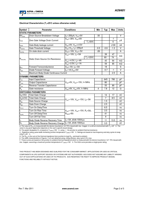
VDS ID (at VGS=-10V) RDS(ON) (at VGS=-10V) RDS(ON) (at VGS =-4.5V) RDS(ON) (at VGS=-2.5V) -30V -5A < 47mΩ < 64mΩ < 85mΩ TSOP6 Top View Bottom View Top View D1 6 D D2 5 D G3 4 S G Pin1 Absolute Maximum Ratings TA=25°C unless otherwise noted Parameter Symbol Drain-Source Voltage VDS Gate-Source Voltage VGS Continuous Drain Current TA=25°C TA=70°C ID Pulsed Drain Current C IDM TA=25°C Power Dissipation B TA=70°C PD Junction and Storage Temperature Range TJ, TSTG Maximum -30 ±12 -5 -4 -28 2 1.3 -55 to 150 Thermal Characteristics Parameter Maximum Junction-to-Ambient A Maximum Junction-to-Ambient A D Maximum Junction-to-Lead t ≤ 10s Steady-State Steady-State Symbol RθJA RθJL Typ 47.5 74 37 Max 62.5 110 50 D S Units V V A W °C Units °C/W °C/W °C/W Rev 7: Mar 2011 www.aosmd.com Page 1 of 5 AO6401 Electrical Characteristics (TJ=25°C unless otherwise noted) Symbol Parameter Conditions Min Typ Max Units STATIC PARAMETERS BVDSS Drain-Source Breakdown Voltage ID=-250µA, VGS=0V -30 IDSS Zero Gate Voltage Drain Current VDS=-30V, VGS=0V TJ=55°C IGSS Gate-Body leakage current VDS=0V, VGS=±12V VGS(th) Gate Threshold Voltage VDS=VGS ID=-250µA -0.5 ID(ON) On state drain current VGS=-10V, VDS=-5V -28 VGS=-10V, ID=-5A RDS(ON) Static Drain-Source On-Resistance VGS=-4.5V, ID=-4A TJ=125°C VGS=-2.5V, ID=-1A gFS Forward Transconductance VDS=-5V, ID=-5A VSD Diode Forward Voltage IS=-1A,VGS=0V IS Maximum Body-Diode Continuous Current V -1 µA -5 ±100 nA -0.9 -1.3 V A 39 47 mΩ 60 74 45 64 mΩ 59 85 mΩ 18 S -0.7 -1 V -2.5 A DYNAMIC PARAMETERS Ciss Input Capacitance Coss Output Capacitance Crss Reverse Transfer Capacitanc
AO6401 30V P-Channel MOSFET General.
| Brand Logo | Part Number | Description | Manufacturer |
|---|---|---|---|
| AO6401 | P-Channel MOSFET | Kexin | |
| AO6401A | P-Channel MOSFET | Kexin |
| Part Number | Description |
|---|---|
| AO6401A | P-Channel MOSFET |
| AO6400 | 30V N-Channel MOSFET |
| AO6402 | 30V N-Channel MOSFET |
| AO6402A | 30V N-Channel MOSFET |
| AO6402L | N-Channel MOSFET |
| AO6403 | 30V P-Channel MOSFET |
| AO6404 | N-Channel MOSFET |
| AO6405 | 30V P-Channel MOSFET |
| AO6407 | P-Channel MOSFET |
| AO6408 | N-Channel MOSFET |