Datasheet Details
| Part number | ICS87973I-147 |
|---|---|
| Manufacturer | IDT |
| File Size | 1.05 MB |
| Description | 1-TO-12 LVCMOS/LVTTL CLOCK MULTIPLIER/ZERO DELAY BUFFER |
| Datasheet |
 ICS87973I-147 Datasheet ICS87973I-147 Datasheet
|
|
|
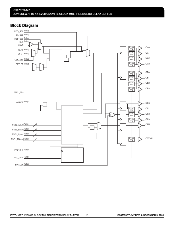
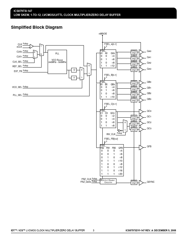
The ICS87973I-147 is a LVCMOS/LVTTL clock generator and a member of the HiPerClockS™family of High Performance Clock Solutions from IDT.
The ICS87973I-147 has three selectable inputs and provides 14 LVCMOS/LVTTL outputs.
The ICS87973I-147 is a highly flexible device.
| Part number | ICS87973I-147 |
|---|---|
| Manufacturer | IDT |
| File Size | 1.05 MB |
| Description | 1-TO-12 LVCMOS/LVTTL CLOCK MULTIPLIER/ZERO DELAY BUFFER |
| Datasheet |
ICS87973I-147 Datasheet
|
|
|
|