Datasheet Details
| Part number | ICS87004I |
|---|---|
| Manufacturer | IDT |
| File Size | 733.10 KB |
| Description | Differential-to-LVCMOS/LVTTL Zero Delay Clock Generator |
| Datasheet |
 ICS87004I Datasheet ICS87004I Datasheet
|
|
|
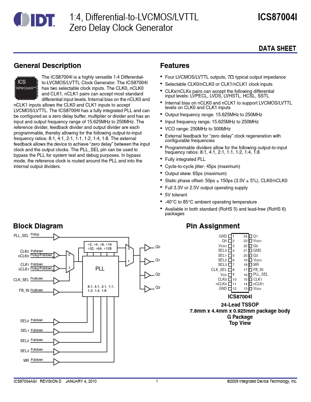
to-LVCMOS/LVTTL Clock Generator.
HiPerClockS™ has two selectable clock inputs.
differential input levels.
| Part number | ICS87004I |
|---|---|
| Manufacturer | IDT |
| File Size | 733.10 KB |
| Description | Differential-to-LVCMOS/LVTTL Zero Delay Clock Generator |
| Datasheet |
ICS87004I Datasheet
|
|
|
|