Datasheet Details
| Part number | ICS87008I |
|---|---|
| Manufacturer | IDT |
| File Size | 277.92 KB |
| Description | 1-TO-8 DIFFERENTIAL-TO-LVCMOS/LVTTL CLOCK GENERATOR |
| Datasheet |
 ICS87008I Datasheet ICS87008I Datasheet
|
|
|
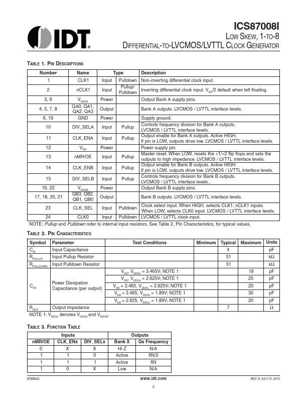
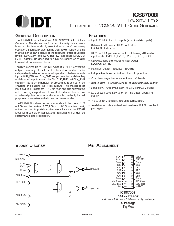
The ICS87008I is a low skew, 1:8 LVCMOS/LVTTL Clock Generator.
The device has 2 banks of 4 outputs and each bank can be independently selected for ÷1 or ÷2 frequency operation.
| Part number | ICS87008I |
|---|---|
| Manufacturer | IDT |
| File Size | 277.92 KB |
| Description | 1-TO-8 DIFFERENTIAL-TO-LVCMOS/LVTTL CLOCK GENERATOR |
| Datasheet |
ICS87008I Datasheet
|
|
|
|