FDC654P Overview
Key Specifications
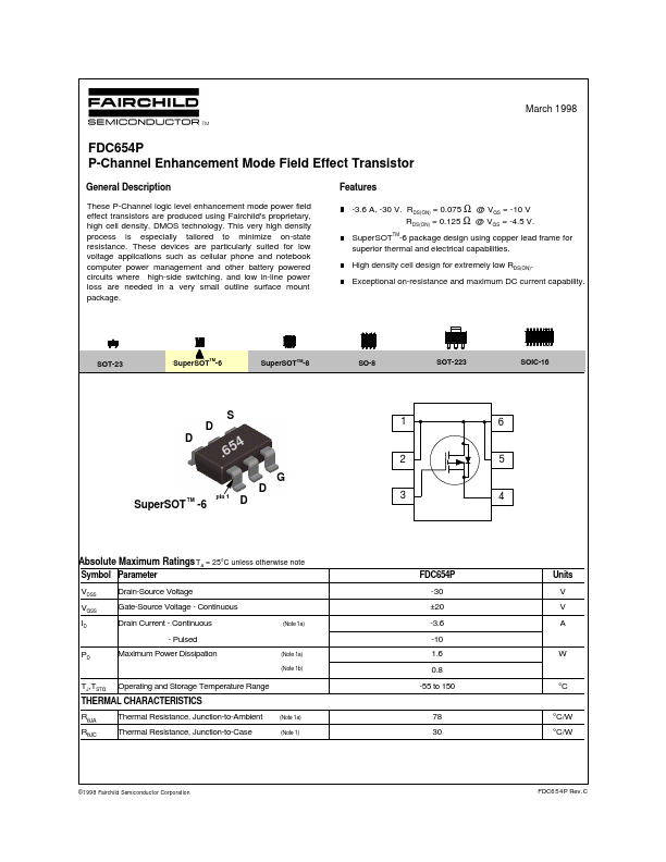
Package: SOT-23-6
Mount Type: Surface Mount
Pins: 6
Height: 1.1 mm
Description
These P-Channel logic level enhancement mode power field effect transistors are produced using Fairchild's proprietary, high cell density, DMOS technology. This very high density process is especially tailored to minimize on-state resistance.
Key Features
- RDS(ON) = 0.075 Ω @ VGS = -10 V RDS(ON) = 0.125 Ω @ VGS = -4.5 V
- SuperSOTTM-6 package design using copper lead frame for superior thermal and electrical capabilities
- High density cell design for extremely low RDS(ON)
- Exceptional on-resistance and maximum DC current capability